Flash Module Control Registers
PRELIMINARY
2-8
PRELIMINARY
2.3 Flash Module Control Registers
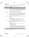
Table 2–2 lists the control registers and their relative addresses within the four
locations that repeat throughout the module’s address range.
Table 2–2. Flash Module Control Registers
Relative
Register
Described in ...
R
e
l
at
i
ve
Address
R
eg
i
ster
Name
Description
Section
Page
0 SEG_CTR Segment control register. The eight MSBs enable spe-
cific segments for programming. Setting a bit to 1 en-
ables the segment. The eight LSBs control the pro-
gram, erase, and verify operations of the module.
2.3.1 2-5
1 TST Test register. Reserved for test; not accessible to the
user.
2.3.2 2-8
2 WADRS Write address register. Holds the address for a write
operation.
2.3.3 2-8
3
WDATA Write data register. Holds the data for a write operation. 2.3.4 2-8
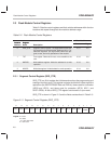
2.3.1 Segment Control Register (SEG_CTR)
SEG_CTR is a 16-bit register that initiates and monitors the programming and
erasing of the flash array. This register contains the bits that initiate the active
operations (the WRITE/ERASE field and EXE bit), those used for verification
(VER0 and VER1), and those used for protection (KEY0, KEY1, and
SEG7–SEG0). All bits of SEG_CTR register are cleared to 0 upon reset.
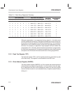
SEG_CTR is shown in Figure 2–3 and the fields are described in Table 2–3.
Figure 2–3. Segment Control Register (SEG_CTR)
15 14 13 12 11 10 9 8 7 6 5 4 3 2 1 0
SEG7 SEG6 SEG5 SEG4 SEG3 SEG2 SEG1 SEG0 Res KEY1 KEY0 VER0 VER1
WRITE/
ERASE
EXE
RW–0 RW–0 RW–0 RW–0 RW–0 RW–0 RW–0 RW–0 X RW–0 RW–0 RW–0 RW–0 RW–0 RW–0
Legend: R = read
W = write
–0 = value after reset
X = don’t care


