


Flash-Write Algorithm
PRELIMINARY
3-15
Algorithm Implementations and Software Considerations
PRELIMINARY
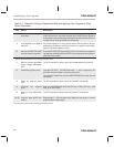
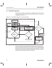
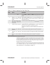
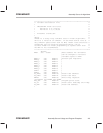
Table 3–3. Steps for Applying One Flash-Write Pulse
Steps Action Description
1 Power up the V
CCP
pin. Set the V
CCP
pin to V
DD
. If the V
CCP
pin for the flash module to be re-
covered is not set to V
DD
, then the flash-write operation will not be ef-
fective.
2 Activate the flash-write
mode and enable all seg-
ments.
Set the WRITE/ERASE field to 10 and set SEG0–SEG7 in the
SEG_CTR register. The flash module must be in register access
mode (see section 2.2).
3 Wait for the internally gener-
ated supply voltage stabi-
lization time.
The CPU executes a delay loop for the t
d(FLW-MODE
†
)
time period.
4 Initiate the flash-write pulse. Load the EXE, KEY1, and KEY0 bits with 1, 1, and 0, respectively. All
three bits must be loaded in the same write cycle.
The segment enable bits and WRITE/ERASE field must also be main-
tained.
5 Delay for the flash-write
pulse time.
The CPU executes a delay loop for the t
d(FLW
†
)
time period.
6 Terminate the flash-write
pulse.
Clear all bits in the SEG_CTR register (load SEG_CTR with 0000h).
7 Delay for mode deselect
time.
CPU executes a delay loop for the t
d(BUSY
†
)
time period.
†
See the device data sheet for the timing parameter values.
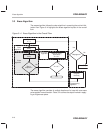
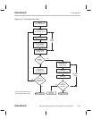
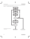
The flash-write algorithm consists of multiple iterations of a loop with one flash-
write pulse applied in each iteration. At the beginning of each iteration, a deple-
tion test is performed to determine if a flash-write pulse is required. Figure 3–7
shows the flow of the flash-write algorithm.
The flash-write operation uses the inverse-erase read mode to detect bits that
are in depletion mode. For more information about the inverse-erase read
mode, see section 2.4,
Read Modes
, on page 2-12.