


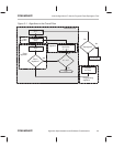
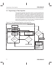
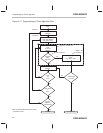

Programming (or Clear) Algorithm
PRELIMINARY
3-7
Algorithm Implementations and Software Considerations
PRELIMINARY
Another important consideration is the total amount of time required to do the
programming. The number of programming pulses required to completely pro-
gram a flash memory cell increases as ambient temperature increases and/or
supply voltage decreases. More programming pulses are required when the
minimum supply voltage is used than when the nominal or maximum supply
voltage is used. The number of program pulses required also increases
throughout the life of the device, as more program-erase cycles are carried
out. The device data sheet specifies the maximum number of program pulses
under all operating conditions; use this number when you calculate the maxi-
mum amount of time required for programming.
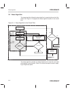
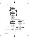
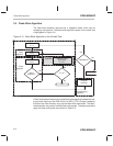
The algorithm incorporates the steps for applying a program pulse (outlined
in Table 3–1) along with some other techniques to ensure margin. In general,
not all flash bits require the same number of program pulses to reach the pro-
grammed margin level. For this reason, the programming algorithm applies a
series of short program pulses until the memory location is programmed. How-
ever, to understand how the series of program pulses works, you must first un-
derstand how the algorithm applies a single program pulse. Table 3–1 outlines
the steps involved in verifying programmed bits and applying a single pulse to
each of the upper and lower bytes of a single location. This process corre-
sponds to the steps enclosed in the dashed box in the flowchart in Figure 3–3.
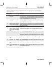
Table 3–1. Steps for Verifying Programmed Bits and Applying One Program or Clear
Pulse
Step Action Description
1 Power up the V
CCP
pin. Set the V
CCP
pin to V
DD.
If the V
CCP
pin for the flash module to be pro-
grammed is not set to V
DD
, then the array will not be programmed.
2 Activate VER0 mode. Set the VER0 bit in SEG_CTR (load SEG_CTR with 0010h).
3 Delay for VER0 reference
voltage stabilization.
The CPU executes a delay loop for the t
d(VERIFY-SETUP
†
)
time period.
4 Read flash array contents for
verification.
The CPU reads the addressed location. The flash module must be in
array-access mode (see section 2.2,
Accessing the Flash Module
, page
2-5).
5 Deactivate VER0 mode. Clear the VER0 bit in SEG_CTR (load SEG_CTR with 0000h).
6 Compare contents of flash
location (16 bits) with de-
sired data.
If the verification passes (i.e., if the data read in step 4 is equal to the de-
sired data value), then no further program pulses are required. The flash
word has been programmed with the desired data value. The program
or clear function is completed and this algorithm is exited.
If the verification fails (i.e., if the data read in step 4 is not equal to the
desired data value), then proceed to step 7.