


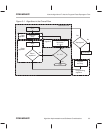
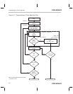
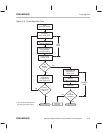


Erase Algorithm
PRELIMINARY
3-11
Algorithm Implementations and Software Considerations
PRELIMINARY
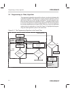
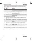
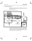
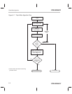
Table 3–2. Steps for Applying One Erase Pulse
Step Action Description
1 Power up the V
CCP
pin. Set V
CCP
pin to V
DD.
If the V
CCP
pin for the flash module to be erased
is not set to V
DD
, then the array will not be erased properly.
2 Load WDATA register with
FFFFh.
This load overrides the erase protection mechanism.
3 Activate the erase mode and
enable segments.
Set the WRITE/ERASE field to 01 and set SEG0–SEG7 bits in the
SEG_CTR register. The flash module must be in register-access
mode (see section 2.2).
4 Wait for internally generated
supply voltage stabilization
time.
The CPU executes a delay loop for the t
d(ERASE-MODE
†
)
time period.
5 Initiate the erase pulse. Load the EXE, KEY1, and KEY0 bits with 1, 1, and 0, respectively. All
three bits must be loaded in the same write cycle.
The segment enable bits and the WRITE/ERASE field must also be
maintained.
6 Delay for erase pulse time. The CPU executes a delay loop for the t
d(ERASE
†
)
time period.
7 Terminate the erase pulse. Clear the EXE bit and WRITE/ERASE field in the SEG_CTR register
(load SEG_CTR with 0000h to clear all bits).
8
Delay for mode deselect
time.
CPU executes a delay loop for the t
d(BUSY
†
)
time period.
†
See the device data sheet for the timing parameter values.
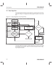
At the beginning of each iteration, a read operation is performed on all the bits
in the array to determine if an erase pulse is required. Erasure is complete
when all array locations are read as FFFFh. To assure that the flash array is
erased with enough margin, the reads associated with the erase use the VER1
read mode. Additional margin can be gained during the erase operation if the
reads are performed using
address complementing
. When the array is read
with address complementing, the following sequence is used for each address
read:
1) All of the bits of the address to be read are complemented.
2) The contents of the resulting address are read.
3) The value read at the complemented address is discarded.