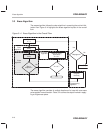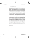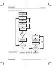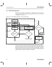
Programming (or Clear) Algorithm
PRELIMINARY
3-8
PRELIMINARY
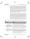
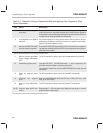
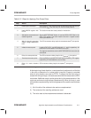
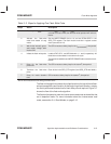
Table 3–1. Steps for Verifying Programmed Bits and Applying One Program or Clear
Pulse (Continued)
Step DescriptionAction
7 Mask the data to program
lower byte.
Mask any bits in the lower byte that do not require programming (are al-
ready read as zero), and mask off upper byte. Recall that the algorithm
should mask one byte while programming the other because a maximum
of eight bits can be programmed simultaneously.
8 Load WADRS and WDATA
registers.
If the flash module is in array access mode, write the data to be pro-
grammed to its address. If the flash module is in register access mode,
load the individual registers directly.
10 Activate the WRITE/ERASE
field and enable segments.
Set the WRITE/ERASE field in SEG_CTR to 10 and set the correspond-
ing segment enable bits (SEG0–SEG7) for the segments where the pro-
grammed word resides.
†
See the device data sheet for the timing parameter values.
11 Wait for internally generated
supply voltage stabilization
time.
The CPU executes a delay loop for the t
d(PGM–MODE
†
)
time period.
12 Initiate the program pulse. Load the EXE, KEY1, and KEY0 bits with 1, 1, and 0, respectively. All
three bits must be loaded in the same write cycle.
The segment enable bits and the WRITE/ERASE field must also be
maintained.
13 Delay for program pulse
time.
The CPU executes a delay loop for the t
d(PGM
†
)
time period.
14 Terminate the program
pulse.
Clear the WRITE/ERASE field and EXE bit in SEG_CTR (e.g., load
SEG_CTR with 0000h).
15 Delay for array stabilization
time.
The CPU executes a delay loop for the t
d(BUSY
†
)
time period.
16–25 Program upper byte if nec-
essary.
Repeat steps 7–15 for the upper byte. Mask the lower byte to 1s when
programming the upper byte.
†
See the device data sheet for the timing parameter values.


