


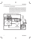
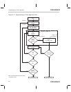
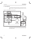

Programming (or Clear) Algorithm
PRELIMINARY
3-5
Algorithm Implementations and Software Considerations
PRELIMINARY
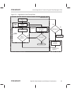
The main feature of the program/clear algorithm is the concept of program-
ming an entire row of bits in a group. The ’F20x/F24x flash array is organized
in rows of 32 words. That is, addresses 0000h through 001Fh are physically
located on the same row of the flash memory array. The array is designed so
that there is a dependence between the charge levels on adjacent (even–odd)
addresses during programming. Programming the bits of an odd address re-
duces the charge margin of the programmed bits (the 0s) in the preceding ad-
jacent (even) address within the row. Similarly, programming the bits of an
even address reduces the charge margin of the programmed bits in the next
adjacent (odd) address within the row. Because of this dependence, if each
address is programmed individually, the charge levels among programmed
bits is not uniform. The programming algorithm improves the uniformity of
charge levels on programmed bits by programming all of the words of a row
in a group. For example, the contents of address 0000h is compared with the
data to be programmed and one program pulse is applied if necessary. The
same procedure is performed on addresses 0001h through 001Fh. The proce-
dure repeats starting at address 0000h until no more program pulses are re-
quired for any address in the row. The number of iterations of this loop equals
the maximum number of program pulse
s
required to program the bits in the
row.
The flow for the programming algorithm is shown in Figure 3–3, and the as-
sembly code is given in Appendix A.
An important consideration for programming the flash array is the CPU fre-
quency range for the application. Because of the actual implementation of the
flash memory circuitry, a 0 bit is most easily read at high frequency; pro-
grammed bits have less margin when read at lower frequency. So, if the ap-
plication requires a variable CPU clock rate, programming should be per-
formed at the lowest frequency in the range. (A similar condition exists for the
erase operation, which requires execution of the erase algorithm at the highest
frequency in the range. See section 3.3, page 3-10.)
Only the read portion of the program operation must be performed at the lower
frequency, because the read is used to determine margin. The read operation
can be extended by sequentially executing multiple reads on the same loca-
tion. Because the same address is selected the entire time and internal control
signals are maintained between reads, the final read is equivalent to a slow
read. For example, if the DSP core is executing the programming algorithm at
a CLKOUT rate of 20 MHz (50 ns), sequentially reading a location three times
is equivalent to reading it once at 6.67 MHz (150 ns). This is important, be-
cause it facilitates execution of the program and erase algorithms at the same
CLKOUT rate.