


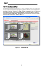


49
ICC
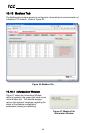
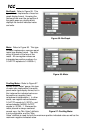
10.10.2 Supervisory Timer Selection
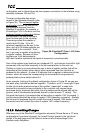
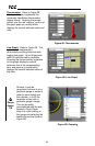
Figure 48 shows the checkbox which enables the
interface card’s Modbus “supervisory timer” function.
This timer provides the ability for the interface card to
monitor timeout occurrences between successive
Modbus TCP socket connections, as opposed to the
standard timeout functionality (refer to section 10.7.5),
which monitors timeout occurrences only within the
scope of each client socket connection. While this feature provides an additional
level of fail-safe functionality for those applications that require it, there are several
ramifications that must be understood prior to enabling this capability. Before
enabling this timer, therefore, it is suggested that users read the ICC whitepaper
titled “A Discussion of Modbus/TCP Server-Side Timeout Processing”, which can be
found in the documents section at http://www.iccdesigns.com.
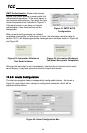
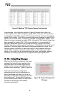
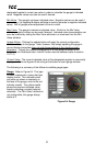
10.10.3 Register Remap Configuration
At times, it may be convenient to access inverter registers in bulk Modbus
transactions. This may be especially true in situations where it is desired to access
certain registers that are natively non-contiguous. For example, if it were desired to
read the inverter’s status 1 word (register 1302), torque (register 1319) and output
voltage (register 1306), this could be accomplished in two different ways:
1. Implement three separate Modbus read transactions, each one reading one
register only, or
2. Implement one single Modbus read transaction, starting at register 1302 for
a quantity of 18 registers. Then, pick out the registers of interest and ignore
the rest of the response data.
While both of these methods will certainly work, neither one of them is optimized for
the task at hand, which is to access three specific register values. A fully optimized
solution can be realized, however, by making use of the interface card’s Modbus
register remapping capabilities. This mechanism operates by allocating a block of 50
user-configurable registers (2001..2050) that remap to other inverter registers. In
this way, non-contiguous inverter registers can be grouped together in any order and
accessed efficiently via the Modbus TCP “read multiple registers” and “write multiple
registers” function codes. The net effect is one of being able to transfer larger blocks
of registers using fewer Modbus transactions, which results in improved network
utilization and simpler data manipulation code on the Modbus master device.
Figure 49 shows the register remap configuration array. Clicking on an entry field in
the “Remaps To” column allows the user to enter an inverter register number that will
then be accessible at the register indicated in the adjacent “Register” column. An
assignment of 0 in the “Remaps To” column indicates that no inverter register is
remapped at that location, which results in written values being ignored and read
values returned as a default value of 0. Note that remapped inverter registers are
still accessible at their original locations: remapping simply provides an additional
means of accessing the original register’s value.
Figure 48: Supervisory
Timer Selection