


Stylus Color service Manual
Appendix
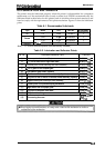
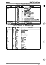
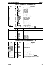
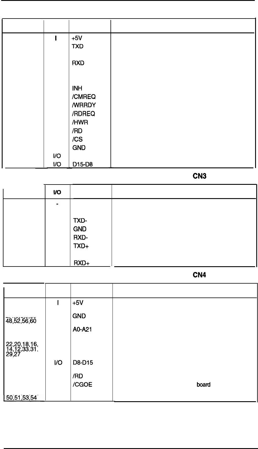
Table A-3. Connector Pin Assignments - CN2
Pin
1-6
7
8
9
10
11
12
13
14
15
16
17
18
19-24
25-28
29-36
Pin
1
2
3
4
5
6
7
8
1
Pin
13,671035,
37,4{,67,69
2,4589,39,
48,~~,~6,60
46,44,42,40,
38,36,34,32
30,28,26,24
z,2g,18,~l,
29;27’
‘ ‘
25,23,21,19,
17,15,13,11
43
55
58.45,47.49.
I/o
I
o
0
I
o
0
0
0
0
0
0
0
.
1/0
1/0
Name
+5V
TXD
/READY
RXD
NC
IRESET
INH
/CMREQ
/WRRDY
/RDREQ
/HWR
/RD
Ics
GND
A3-AO
D15-D8
Description
Power supply for l/F drive
Transmit data
Ready signal
Receive data
Not connected
Reset signal
Inhabit signal
Command request signal
Wriie ready signal
Read request signal
High write signal
Read signal
Chip select signal
Ground
Address bus signal 3-O
Data bus signal 15-8
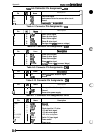
Table A-4. Connector Pin Assignments -
CN3
1/0
.
0
I
o
I
Name
DTR
NC
TXD-
GND
RXD-
TXD+
NC
RXD+
Description
Data terminal ready
Not connected
Transmit data-
Ground
Receive data -
Transmit data+
Not connected
Receive data +
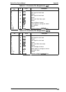
Table A-5. Connector Pin Assignments -
CN4
I/o
I
o
1/0
o
0
0
Name
+5V
GND
AO-A21
D8-D15
/RD
ICGOE
/CG
Description
Power supply for option CG
Ground
Address signal 0-21
Data bus signal 8-15
Read signal for CG board
Output enable CG ROM on CG
board
CG ROM output enable signal on CG board
(Memory select signal)
Rev. A
A-3