


Appendix
Stykiscakw
Swvbehtmud
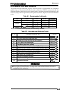
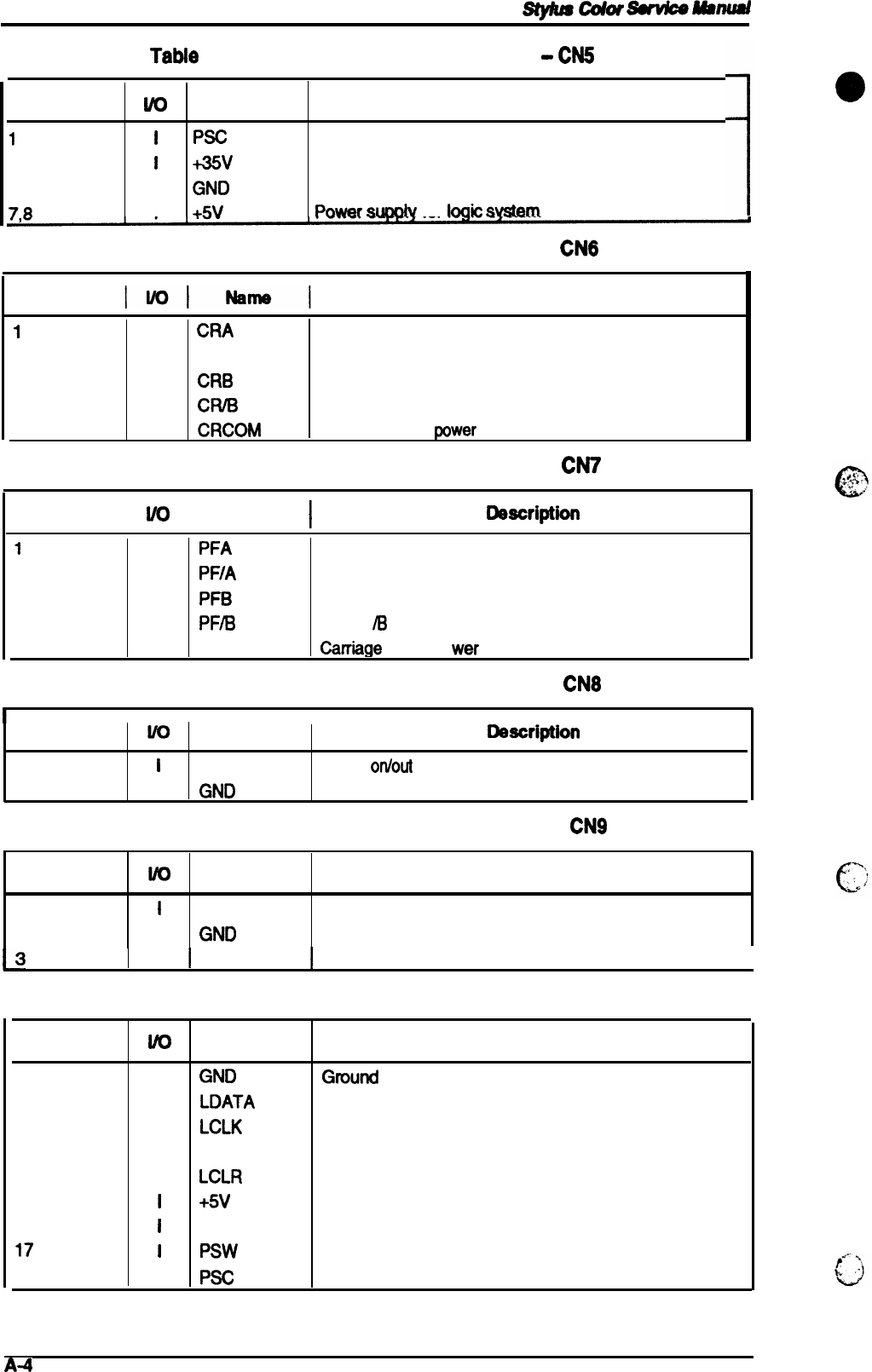
Table
A-6.
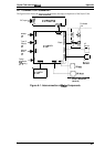
Connector
Pin Assignments
-
CN5
Pin
w
Name
Description
1
I
Psc
Power scan signal
2,3
I
&v
Head common driver for common drive circuit
4-6
GND
Ground
7n
I
4-W
Pmuer
sumtv for
Ioaic
svstem
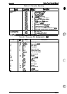
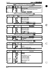
Table
A-7.
Connector
Pin Assignments -
CN6
Pin
Description
1
0
CRA
Phase A drive signal
2
0
CR/A
Phase /A drive signal
3
0
CRB
Phase B drive signal
4
0
cm
Phase /B drive signal
5
0
CRCOM Carriage drive
PO
wer
(common voltage)
Table A-8. Connector Pin Assignments -
CN7
Pin
I
I/o
I
Name
I
i)esoription
1
0
PFA Phase A drive signal
2
0
PF/A Phase /A drive signal
3 0
PFB Phase B drive signal
4
0
PF/B Phase
/El
drive signal
5
0
PFCOM
Camiage
drive
PO
wer
(common Wage)
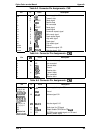
Table A-9. Connector
Pin Assignments -
CN8
Pin
m
Name
iMcription
1
I
PE
Paper
otiout
state detection signal
2
.
GND Ground
Table
A-10. Connector Pin Assignments -
CN9
Pin
m
Name
Description
1
I
HP
Home position detection signal
2
.
GND
Ground
13
0
I
HPV
I
Sensor drive power supply
I
Table
A-1 1. Connector Pin Assignments- CN1O
Pin
I/o
Name
Description
1,3,5,7
.
GND
Ground
2
0
LDATA
LED data
4
0
LCLK
Clock signal for
LED
drive
6
0
LLAT
LED
data latch signal
8
0
LCLR
LED
data reset signal
9,11,19,20
I
+5V
LED driver and power
10,12-16
I
SWO-5
Switch O-5 input signal
17
I
Psw
Power switch
18
I
Psc
Power scan
A4
Rev. A