


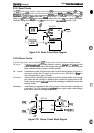
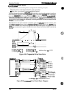
Operating Principles
Stylus
C&w
SW*
hhnual
2S.2.5
Printhead
Drive Circuit
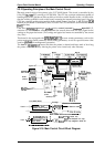
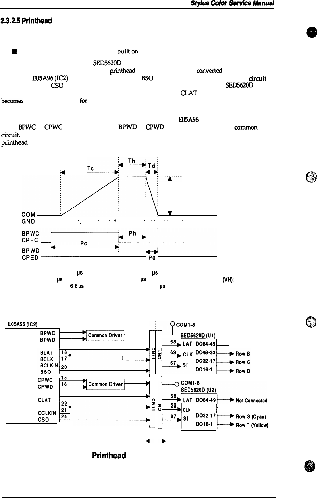
The pnnthead drive circuit for this printer is composed of the following two parts:
■
Common drive circuit (trapezoidal drive pulse generation)
H
Head drive circuit (nozzle control
built~
theprinthead)
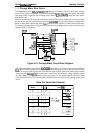
The W-bit thermal head driver
SED5620D
in the head drive circuit on the carriage is used as a
nozzle selector to selectively drive the
printhead
nozzles. Print data is
mwerted
into serial data by
gate array
E05A96
(IC2)
and is output from port
BSO
(pin 20) to the black head
drive
arcuit or
output from port
CSO
(pin 24) to the
color head drive circuit. Then, head driver
SED5620D
latches
the head data when gate array E05A96BA outputs the BLAT or
CLAT
signal, and the latched data
komes
64-bit parallel
data
fix
the black head, or 48-bit parallel data for the color head. One bit
corresponds to each nozzle.
When data
transfix and nozzle selection is complete, gate array
E05A96
outputs the co
mrnon drive
pulse
BPWC
or
CPWC
(charge pulse) and
BPWD
or
CPWD
(discharge pulse) to the ~mmon drive
arcuit.
The common drive circuit then generates the trapezoidal pulse and applies it to the
printhead
as a co
mmon drive pulse. After this, the nozzle selected by the head data is activated to
inject ink.
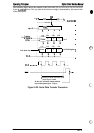
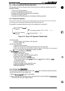
4
VH
*
GND
----------------------
-
.
-
. . . . . . . . . .
-
. . . . .
-
. .
.:.
. . . . . . . .
-
. . . . . .
.
. . .
-
.
.-
. .
-
.
-
.
-
-
-
- - - . -
-
- . . . - - . - - - - -- - - -
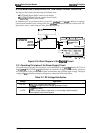
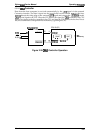
CPEC
*
BPWD
CPED
Tc: Charge time 82-88
w
Pc: Charge pulse 92
IJS
Th: Idle time 3
ps
Ph: Idle pulse 2
IJS
Head drive
voltage
(VH):
16-26 V
Td: Discharge time
6,6
IJS
Pd: Discharge
pulse
10
PS
Figure 2-24. Trapezoidal Drive Wave Form
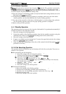
E05A96
(IC2)
COMI-8
BPWC
‘;:
●
SED5620D
(Ul)
BPWD
19
●
Row A
14C
I
1
I
I
I
CPWC
CPWD
CLAT
CCL’
CCLKIN
Cso
b“
23
m
-1
1-
C137 MAIN
-
s2RH-Notconnected
I--d
z
69
0
CLK
0048-33
●
Row R (Magenta)
~
On
Carriage
(Head
Driver
Board)
2-25.
Printhead
Drive Circuit Block Diagram
Figure
2-20
Rev. A
c)
+*->
*