


Op8fsthg Pfincipks
stylus
Coiaf
~mnwl
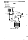
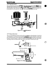
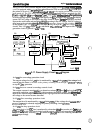
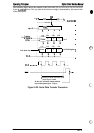
The
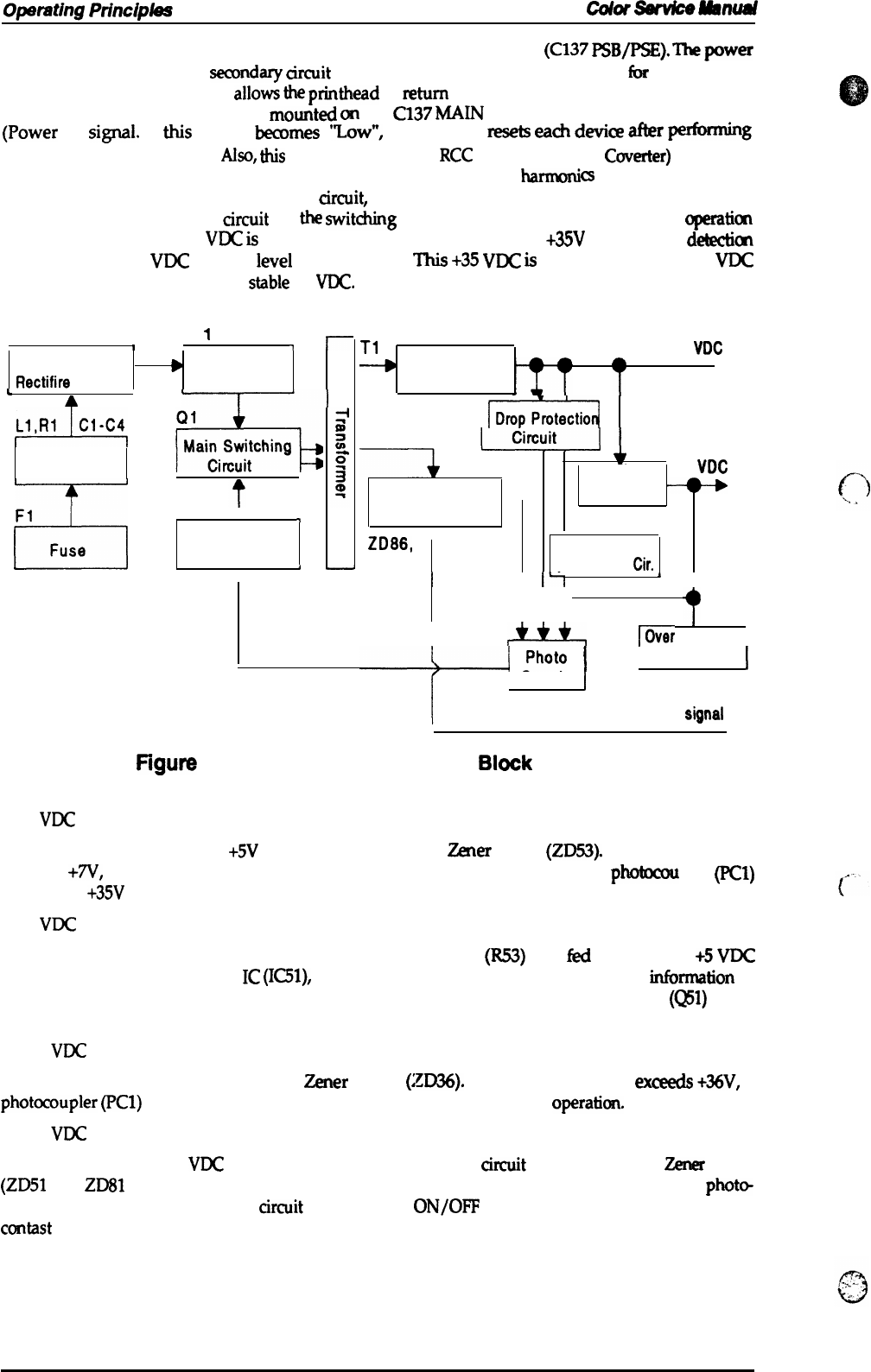
figure below
shows a block diagram of the power supply
circuit
(C137
PSB/PSE).
The
POW=
switch
is equipped with a
semndary
*it
that allows the CPU to remain active
fbr
a while after
the printer is
turned off. This
allows
the
printkad
to
return
to the capping position after power has
been turned off. The CPU that is rnowted
CXI
the
C137
MAIN
board always monitors the PSC
(Power
@/
~
sipl.
If
w
signal
bemmes
‘ZOW”,
the CPU
resets
-*
device
*
-g
the
head capping sequence.
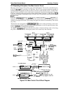
Nw,
this
board employs the
RCC
(Ringing Choke
Coverter)
switching
system. This AC voltage is first input to the filter circuit for higher
harmoni
cs
absorption, and then
input to the rectification and smoothing
arcuit,
converting it into DC voltage. This DC voltage is
then input to the switching
arcuit
for
the
swittig
operation. Along with the switching
operatim
on the primary
side, +35
WC
is
generated after passing through the
+35V
line voltage
detectim
circuit. This +35
VDC
output
level
is stabilized.
This
+3S
VDC
is
also input to the +5
VDC
generation circuit to generate a
stable
+5
VDC.
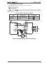
DB1
cl
1
1
1
r
Full-wave
b
Smoothing
Rectifire
Circuit
Circuit
L
I
A
—-T----1
W-@
Filter Circuit
d
F1
Fuse
F+13
I
7
Feed back
Circuit
)
4
C51
T1
Smoothing
+35
Voc
*
➤
Circuit
ZD51 , 81-84
~~
‘
+5
VDC
P-off Detection
TL 494
and delay circuit
A
ZD52
ZD86,
Over voltage
C82
protection
Cir.
I
I
1’”1
4
I
I It
ZD53
,
I
[Over
voltage
I
~
‘hot?
I
[protection Cir.
[
[
I
Coupler
I
Pcl
P-OFF
signal
Hgure
2-17. Power Supply Circuit
Biock
Diagram
1)+5
VDC
line overvoltage protection circuit
The output voltage level of
+5V
line is monitored by a
Zener
diode
(ZD53). If the voltage
level
exceeds
+7V,
the status
is fed back to the primary switching circuit through a
photocou
pier
(-WI)
to stop the
+35V
generation.
2)+5
VDC
line over current/ overvoltage control circuit.
The output current is monitored by a detection resistor
(R53)
and
M
back to the
+5
VDC
generation switching control
IC
(IC51),
which monitors the output voltage. This
inhmation
is
input to the internal comparator and outputs the high signal to turn off the transistor
(QW)
when
the voltage or the current becomes abnormal.
3) +35
VDC
line overvoltage protection circuit
The output level is monitored by a
Zener
diode
(ZD36).
If the voltage level
excwds
+36V,
a
photocoupler
(PCl)
is activated; stopping the primary switching circuit
operatim.
4) +35
VDC
line drop protection circuit
The output level of +35
VDC
line is monitored by a detection
arcuit
that consists of a
Zener
diode
(ZD51
and
ZD81
to 84). This circuit feeds back the output voltage level status through a
photm
coupler to the primary switching arcuit to control the
ON/OPP
time of the switching transistor for
contast
output voltage.
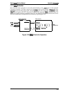
2-14
Rev.
A