


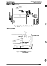
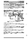
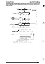
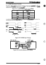
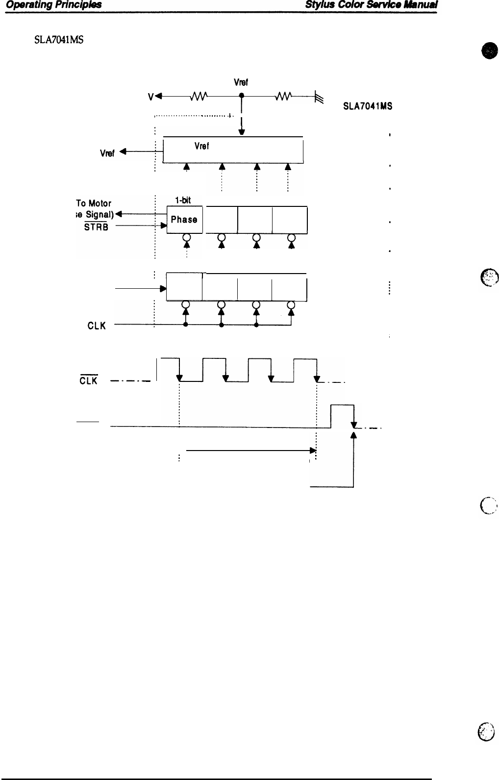
The following figure shows the contents of the 4-bit serial
data and how these data are transacted
by the
SLA7041MS
driver. The step time of the reference voltage is determined by the interval time
of the strobe pulse.
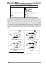
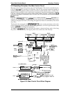
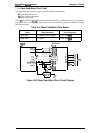
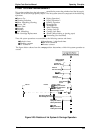
+5
W8f
v+
a
SLA7041MS
0-------------------
----------
-L.
-------------------- -------------------- ------------
I
v-+-l
Vref
Voltage Selection
Circuit
‘=r*
(Phase Signal)
1-bit
;r————T—
2-bit 3-bit 4-bit
a
b
c
Latch
2-bit 3-bit
4-bit
I
.
.
.
.
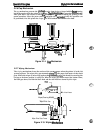
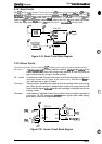
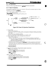
4-bit Serial Data
*
Phase
a
b
c
4-bit Shift Register
~
h
.
.
CLK
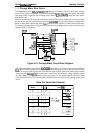
. . . . . . . . . . . . . . . . . . . . . . . . . . . . . . . . . . . . . . . . . . . . . . . . . . . . . . . . . . . . . . . . . . . . . . . . . . . . . . . . . . . .
.
CLK
–-–-–
STRB
-—.
4
L1
~
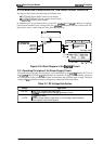
Reading of serial data from the
:
phase signal
in order
At this time, reference voltage selection
circuit checks phase
signal outputs
Figure 2-22. Serial Data Transfer Procedure
2-18
Rev. A