S1C63558 TECHNICAL MANUAL EPSON 137
CHAPTER 4: PERIPHERAL CIRCUITS AND OPERATION (FSK Demodulator)
Band-pass
filter
Carrier
detection circuit
Reference voltage
generation circuit
TIP
Amp
–
+
AV
SS
AV
DD
FSKIN
CDET
RDET
FOSC3
PWDN
RDIN
RING
FB
0.1µF
RDRC
V
REF
V
DD
BPOUT
CDIN
FSK
demodulator
Clock
generator
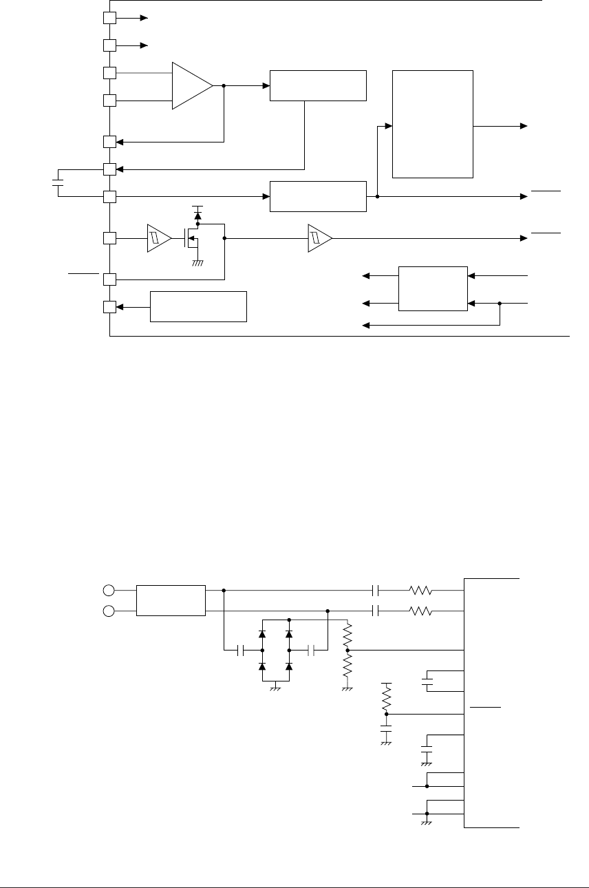
Fig. 4.15.1.2 FSK core configuration
The external terminals of the FSK demodulator are as follows:
AV
DD, AVSS Power terminals for the FSK block. Supply power respectively as AVDD = VDD, AVSS = VSS.
TIP Inverted input terminal of the input amplifier
RING Non-inverted input terminal of the input amplifier
FB Feedback output terminal of the input amplifier
BPOUT Output terminal of the band-pass filter
CDIN Input terminal for carrier signal detection
RDIN Input terminal for ring signal detection
RDRC I/O terminal for connecting an RC network
V
RFF Reference voltage (1/2VDD) output terminal
The basic external connection diagram is shown in Figure 4.15.1.3.
TIP
RING
FB
TIP
RING
RDIN
BPOUT
CDIN
RDRC
Protection
Network
0.2µF 0.2µF
470k
33k
10k1000pF
1000pF
0.2µF
0.1µF
270k
10k
VREF
AVDD
VDD
AVSS
VSS
0.1µF
VDD
Fig. 4.15.1.3 Basic external connection diagram (example for Bellcore)


