


S1C63558 TECHNICAL MANUAL EPSON 87
CHAPTER 4: PERIPHERAL CIRCUITS AND OPERATION (Serial Interface)
(4) Parity bit selection
When checking and adding parity bits, write "1" into the parity enable register EPR to set to "with
parity check". As a result of this setting, in the 7-bit asynchronous mode, it has a 7 bits data +
parity bit configuration and in the 8-bit asynchronous mode it has an 8 bits data + parity bit
configuration.In this case, parity checking for receiving and adding a party bit for transmitting is
done automatically in hardware. Moreover, when "with parity check" has been selected, "odd" or
"even" parity must be further selected in the parity mode selection register PMD.
When "0" is written to the PMD register to select "without parity check" in the 7-bit asynchronous
mode, data configuration is set to 7 bits data (no parity) and in the 8-bit asynchronous mode (no
parity) it is set to 8 bits data (no parity) and parity checking and parity bit adding will not be done.
(5) Clock source selection
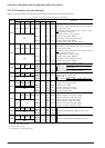
Select the clock source by writing data to the two bits of the clock source selection registers SCS0
and SCS1. (See Table 4.11.4.1.)
(6) Clock source control
When the programmable timer is selected for the clock source, set transfer rate on the programma-
ble timer side. (See "4.10 Programmable Timer".)
When the divided signal of OSC3 oscillation circuit is selected for the clock source, be sure that the
OSC3 oscillation circuit is turned ON prior to commencing data transfer. (See "4.3 Oscillation
Circuit".)
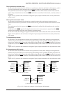
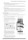
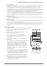
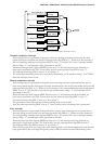
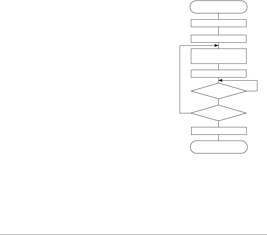
Data transmit procedure
The control procedure and operation during transmitting is as follows.
(1) Write "0" in the transmit enable register TXEN to reset the
serial interface.
(2) Write "1" in the transmit enable register TXEN to set into
the transmitting enable status.
(3)
Write the transmitting data into TRXD0–TRXD7.
Also, when 7-bit data is selected, the TRXD7 data be-
comes invalid.
(4) Write "1" in the transmit control bit TXTRG and start
transmitting.
This control causes the shift clock to change to enable and
a start bit (LOW) is output to the SOUT terminal in
synchronize to its rising edge. The transmitting data set
to the shift register is shifted one bit at a time at each
rising edge of the clock thereafter and is output from the
SOUT terminal. After the data output, it outputs a stop
bit (HIGH) and HIGH level is maintained until the next
start bit is output.
The transmitting complete interrupt factor flag ISTR is set
to "1" at the point where the data transmitting is com-
pleted. When interrupt has been enabled, a transmitting
complete interrupt is generated at this point.
Set the following transmitting data using this interrupt.
(5) Repeat steps (3) to (4) for the number of bytes of trans-
mitting data, and then set the transmit disable status by
writing "0" to the transmit enable register TXEN, when
the transmitting is completed.
Data transmitting
End
TXEN ← 0
No
Yes
Transmit complete ?
Set transmitting data
to TRXD0–TRXD7
No
Yes
ISTR = 1 ?
TXEN ← 0
TXTRG ← 1
TXEN ← 1
Fig. 4.11.7.2 Transmit procedure in
asynchronous mode