


14 EPSON S1C63558 TECHNICAL MANUAL
CHAPTER 4: PERIPHERAL CIRCUITS AND OPERATION (Memory Map)
CHAPTER 4
P
ERIPHERAL
C
IRCUITS
AND
O
PERATION
The peripheral circuits of S1C63558 (timer, I/O, etc.) are interfaced with the CPU in the memory
mapped I/O method. Thus, all the peripheral circuits can be controlled by accessing the I/O memory on
the memory map using the memory operation instructions. The following sections explain the detailed
operation of each peripheral circuit.
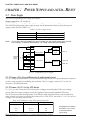
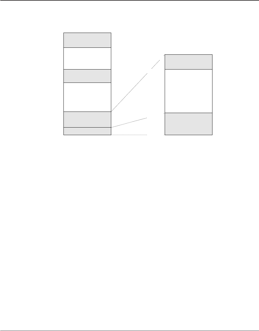
4.1 Memory Map
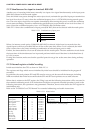
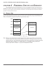
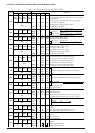
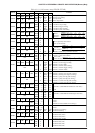
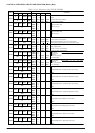
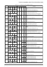
The S1C63558 data memory consists of 5,120-word RAM, 2,048-word data ROM, 816-bit display memory
and 97-word peripheral I/O memory. Figure 4.1.1 shows the overall memory map of the S1C63558, and
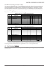
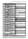
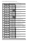
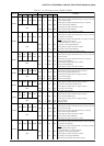
Tables 4.1.1(a)–(h) the peripheral circuits' (I/O space) memory maps.
0000H
1400H
8000H
8800H
F000H
FF00H
FFFFH
RAM area
Unused area
Unused area
Data ROM area
I/O memory area
Display memory area
Unused area
Peripheral I/O area
F000H
F25EH
FF00H
FFFFH
Fig. 4.1.1 Memory map
Note: Memory is not implemented in unused areas within the memory map. Further, some non-imple-
mentation areas and unused (access prohibition) areas exist in the display memory area and the
peripheral I/O area. If the program that accesses these areas is generated, its operation cannot be
guaranteed. Refer to Section 4.7.5, "Display memory", for the display memory, and the I/O
memory maps shown in Tables 4.1.1 (a)–(h) for the peripheral I/O area.