


162 EPSON S1C63558 TECHNICAL MANUAL
CHAPTER 7: ELECTRICAL CHARACTERISTICS
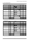
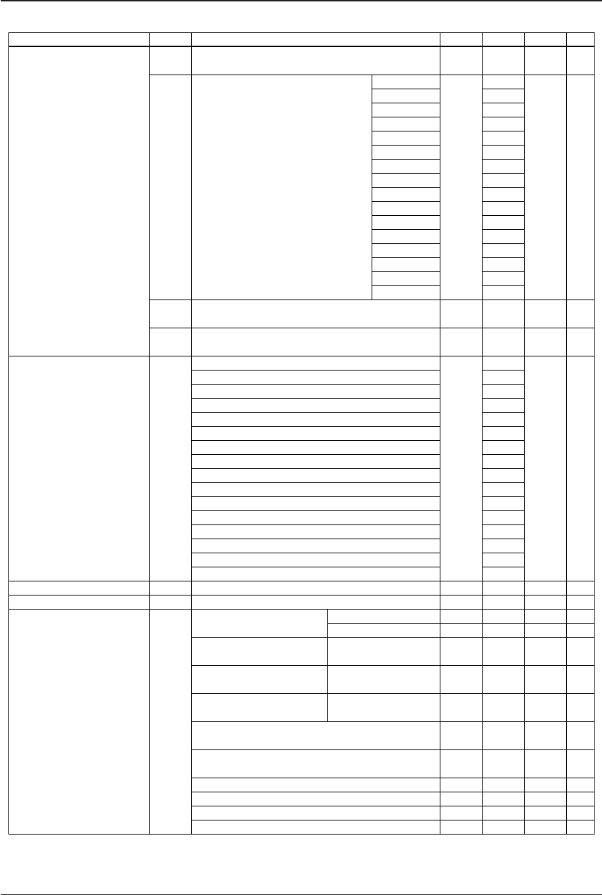
7.4 Analog Circuit Characteristics and Power Current Consumption
Item
LCD drive voltage
Symbol
V
C1
V
C23
V
C4
V
C5
Unit
V
V
V
V
Max.
1/2·V
C23
-0.1
Typ.
×1.12
3/2·V
C23
2·V
C23
Typ.
1.95
1.98
2.01
2.04
2.07
2.10
2.13
2.16
2.19
2.22
2.25
2.28
2.31
2.34
2.37
2.40
Min.
1/2·V
C23
×0.95
Typ.
×0.88
3/2·V
C23
×0.95
2·V
C23
×0.95
Condition
Connect 1 MΩ load resistor between V
SS
and V
C1
(without panel load)
Connect 1 MΩ load resistor LC0–3="0"
between V
SS
and V
C23
LC0–3="1"
(without panel load) LC0–3="2"
LC0–3="3"
LC0–3="4"
LC0–3="5"
LC0–3="6"
LC0–3="7"
LC0–3="8"
LC0–3="9"
LC0–3="10"
LC0–3="11"
LC0–3="12"
LC0–3="13"
LC0–3="14"
LC0–3="15"
Connect 1 MΩ load resistor between V
SS
and V
C4
(without panel load)
Connect 1 MΩ load resistor between V
SS
and V
C5
(without panel load)
Unless otherwise specified:
V
DD
=3.0V, V
SS
=0V, f
OSC1
=32.768kHz, C
G
=25pF, Ta=-20 to 70°C, V
D1
/V
C1
/V
C23
/V
C4
/V
C5
are internal voltage, C
1
–C
7
=0.2µF
SVD voltage
(Ta=25°C)
SVD voltage (external) ∗3
SVD circuit response time
Current consumption
(Ta=25°C)
∗1
∗2
∗3
∗4
V
SVD1
V
SVD2
t
SVD
I
OP
V
V
µs
µA
µA
µA
µA
µA
µA
µA
mA
mA
mA
mA
Typ.
×1.07
1.05
100
3
8
19
300
800
15
6
2.5
2.0
2.5
1.5
2.20
2.20
2.20
2.20
2.20
2.30
2.40
2.50
2.60
2.70
2.80
2.90
3.00
3.10
3.20
3.30
0.95
1.5
4
10
150
600
1.4
1.2
1.8
1.0
Typ.
×0.93
0.85
1
0.5
Without panel load. The SVD circuit is OFF.
OSCC = "0"
Please input the voltage, which is within the range between V
SS
and V
DD
, into the SVD terminal.
OSC3 oscillation current and CPU operating current with a 3.58 MHz clock are included.
SVDS0–3="0" (internal)
SVDS0–3="1"
SVDS0–3="2"
SVDS0–3="3"
SVDS0–3="4"
SVDS0–3="5"
SVDS0–3="6"
SVDS0–3="7"
SVDS0–3="8"
SVDS0–3="9"
SVDS0–3="10"
SVDS0–3="11"
SVDS0–3="12"
SVDS0–3="13"
SVDS0–3="14"
SVDS0–3="15"
SVDS0–3="0" (external), Ta = 25°C
Ta = 25°C
During HALT
(32 kHz crystal oscillation)
During execution
(32 kHz crystal oscillation)
During HALT
(3.58 MHz ceramic oscillation)
During execution
(3.58 MHz ceramic oscillation)
SVD circuit current (during supply voltage detection)
V
DD
=2.2 to 5.5 V
SVD circuit current (during external voltage detection)
V
DD
=2.2 to 5.5 V
DTMF circuit current V
DD
=5.5 V ∗4
DTMF circuit current V
DD
=3.0 V ∗4
FSK circuit current V
DD
=5.5 V ∗4
FSK circuit current V
DD
=3.0 V ∗4
LCD power OFF ∗1, ∗2
LCD power ON ∗1, ∗2
LCD power ON ∗1, ∗2
LCD power ON ∗1
LCD power ON ∗1