S1C63558 TECHNICAL MANUAL EPSON 165
CHAPTER 7: ELECTRICAL CHARACTERISTICS
7.7 FSK Demodulator Characteristics
Unless otherwise specified:
VDD=5.0V, VSS=0V, fCLK=3.579545MHz, Ta=-20 to 70°C
Item
Transfer rate
Bell202 mark (logic 1)
frequency
Bell202 space (logic 0)
frequency
ITU-T V.23 mark (logic 1)
frequency
ITU-T V.23 space (logic 0)
frequency
Signal-to-noise ratio
Band-pass filter gain ∗1
Carrier detection ON
sensitivity ∗2
Carrier detection OFF
sensitivity ∗2
Input clock frequency
Input AC impedance
FSKON set-up time
Carrier detection response
time
∗1
∗2
Symbol
T
RATE
fB1
fB0
fV1
fV0
SNR
GBPF
CDON
CDOFF
fCLK
RIN
tSUP
tCDON
tCDOFF
Unit
Baud
Hz
Hz
Hz
Hz
dB
dB
dB
dB
dB
dB
dB
dB
dBm
dBm
MHz
kΩ
ms
ms
ms
Max.
1212
1212
2222
1320
2132
–
–
–
–
–
–
–
–
-48
–
+0.1%
130
–
9
10
Typ.
1200
1200
2200
1300
2100
–
9.2
42.7
42.8
42.7
22.4
3.7
-20.0
-51
-54
3.579545
100
–
6.25
7.5
Min.
1188
1188
2178
1280
2068
20
–
–
–
–
–
–
–
–
-57
-0.1%
70
20
3
5
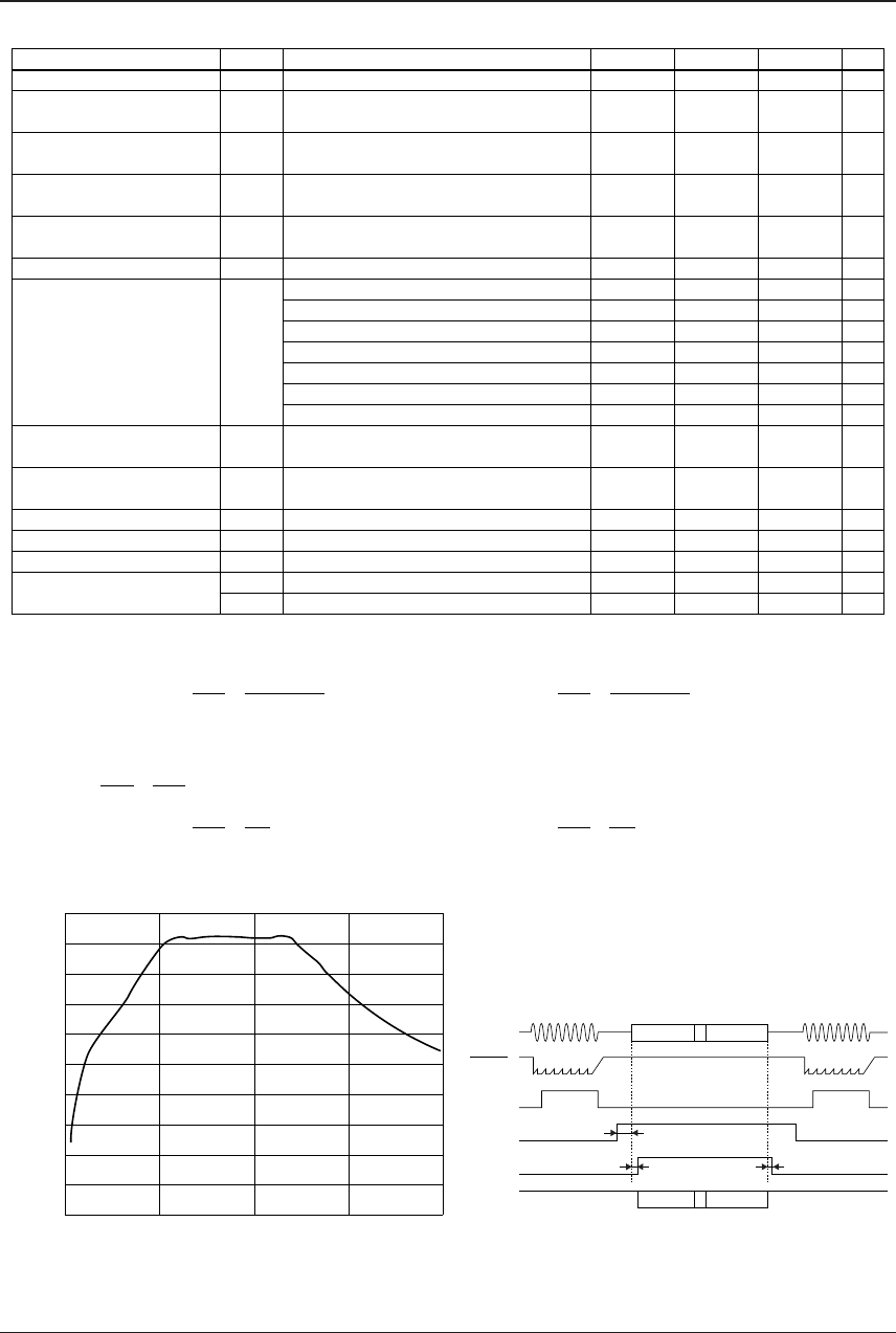
Value measured between TIP/RING pin and BPOUT pin
The following expressions can be used to calculate the typical values (dBm) of CD
ON and CDOFF when an external resistor
RTR (10kΩ Typ.) is connected in series with the TIP pin and the RING pin.
In addition, the following expressions can be used to calculate the sensitivity of CDON and CDOFF when an external feedback
resistor is used for the input amplifier (mask option).
Condition
300Hz
1200Hz
1700Hz
2200Hz
3000Hz
4000Hz
≥10000Hz
V
DD=5.0V
V
DD=5.0V
VDD=5.0V (between TIP/RING pin and VREF)
CDON = -51 + 20log( [dBm] [dBm])×
V
DD
5
100k
R
TR + 100k
CDOFF = -54 + 20log( )×
V
DD
5
100k
R
TR + 100k
CDON = -51 + 20log( [dBm])×
V
DD
5
R1
R5
[dBm])
R
1
R5
GAmp = (R1 = R2, R3 = R4, R5 = R6, see Figure 4.15.2.2.)=
R
5
R1
R6
R2
CDOFF = -54 + 20log( ×
V
DD
5
Band-pass filter gain (Typ. value) Timing chart
50
40
30
20
10
0
-10
-20
-30
-40
-50
Gain (dB)
Frequency (Hz)
0 1000 2000 3000 4000
101010... DATA1
101010... DATA1
1st RING
t
SUP
t
CDON
t
CDOFF
Input
RDRC
RDET
FSKON
CDET
FSKIN
2nd RING
