140 EPSON S1C63558 TECHNICAL MANUAL
CHAPTER 4: PERIPHERAL CIRCUITS AND OPERATION (FSK Demodulator)
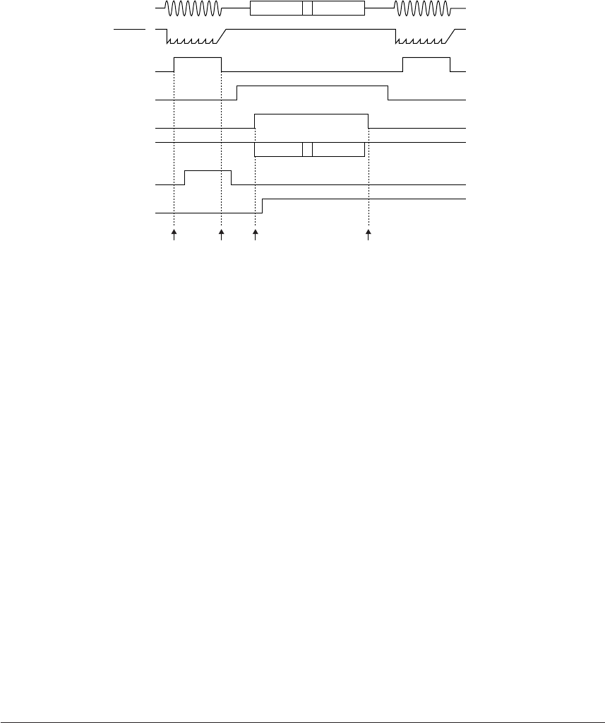
Since the value of both RDIT and CDET is the same as the comparison register, an interrupt does not
occur at (1). When a ring is input, the ring detection interrupt will be generated since RDIT changes "0" to
"1" and no longer matches the contents of RDETCP at (2). To generate an interrupt when a ring input is
completed, write "1" to RDETCP. Copying the RDET bit to RDETCP changes the interrupt timing so that
the interrupt will occur when the RDET changes from the current status. In Figure 4.15.3.1, the RDET bit
has been copied to RDETCP immediately after (2), so an interrupt occurs again when RDET returns from
"1" to "0".
As the same as ring detection interrupt, the carrier detection interrupt will be generated at (4) and (5)
since no matching occurs between CDET and CDETCP.
Figure 4.15.3.2 shows the timing chart for the interrupt generation (example for Bellcore).
101010... DATA1
101010... DATA1
1st RING
Input
RDRC
RDET
FSKON
CDET
FSKIN
RDETCP
CDETCP
Interrupt
2nd RING
(2) (3) (4) (5) ...Step of Figure 4.15.3.1
Fig. 4.15.3.2 Timing chart for interrupt generation (example for Bellcore)
4.15.4 Inputting FSK data
The FSK demodulator starts operating when "1" is written to FSKON (FF66H•D3). Normally it should be
set to "0" to decrease current consumption if not necessary.
The following settings are necessary before starting the FSK demodulator operation.
(1) Setting the serial interface (2)
The demodulated data is loaded to the data register of the serial interface (2).
Therefore, transfer conditions (transfer rate, bit width, parity condition) must be set before receiving
FSK data.
When the FSK demodulator is turned ON (FSKON = "1"), the input line of the serial interface (2) is
switched from P30 to the FSK demodulator output. The I/O terminals (P30–P33) including P30, used
for the serial interface (2), functions as the general I/O port terminals while FSKON is "1".
Refer to Section 4.11, "Serial Interface", for controlling the serial interface (2).
(2) Controlling the OSC3 oscillation circuit
The FSK demodulator uses the OSC3 clock as the operating clock. Therefore, the OSC oscillation
circuit must be turned ON and the CPU operating clock must be switched to OSC3.
It takes a maximum 5 msec for oscillation stabilization after turning the OSC3 oscillation circuit ON.
Do not turn the FSK demodulator ON in this period. Refer to Section 4.3, "Oscillation Circuit", for
controlling the OSC3 oscillation circuit.


