


S1C63558 TECHNICAL MANUAL EPSON 77
CHAPTER 4: PERIPHERAL CIRCUITS AND OPERATION (Serial Interface)
4.11 Serial Interface
4.11.1 Configuration of serial interface
The S1C63558 incorporates 2 channels (SIF (1), SIF (2)) of full duplex serial interface circuits (when
asynchronous system is selected) that allows the user to select either clock synchronous system or
asynchronous system.
The data transfer method can be selected in software.
When the clock synchronous system is selected, 8-bit data transfer is possible.
When the asynchronous system is selected, either 7-bit or 8-bit data transfer is possible, and a parity
check of received data and the addition of a parity bit for transmitting data can automatically be done by
selecting in software.
Differences between SIF (1) and SIF (2)
SIF (1) and SIF (2) are independently separated serial interface blocks that have the same functions and
circuit configurations. The serial I/O terminals and control registers are assigned as follows:
Serial I/O terminals: SIF (1) → P10–P13
SIF (2) → P30–P33
Control register addresses: SIF (1) → FF70H–FF75H, FFE3H, FFF3H
SIF (2) → FF58H–FF5DH, FFE8H, FFF8H
To distinguish the control bits of SIF (1) from SIF (2), "S" is added to the end of the name for the SIF (2)
control bits.
Example: SIF (1) → ESIF, SIF (2) → ESIFS
When using the FSK demodulator, SIF (2) is used for data input. SIF (1) cannot be used for this purpose.
Note: Explanation made in this section is only for SIF (1). Be aware that "S" for the SIF (2) control bits is
omitted. Further, the serial I/O terminal names are explained using P10–P13.
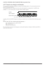
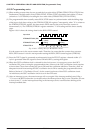
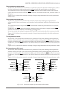
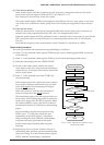
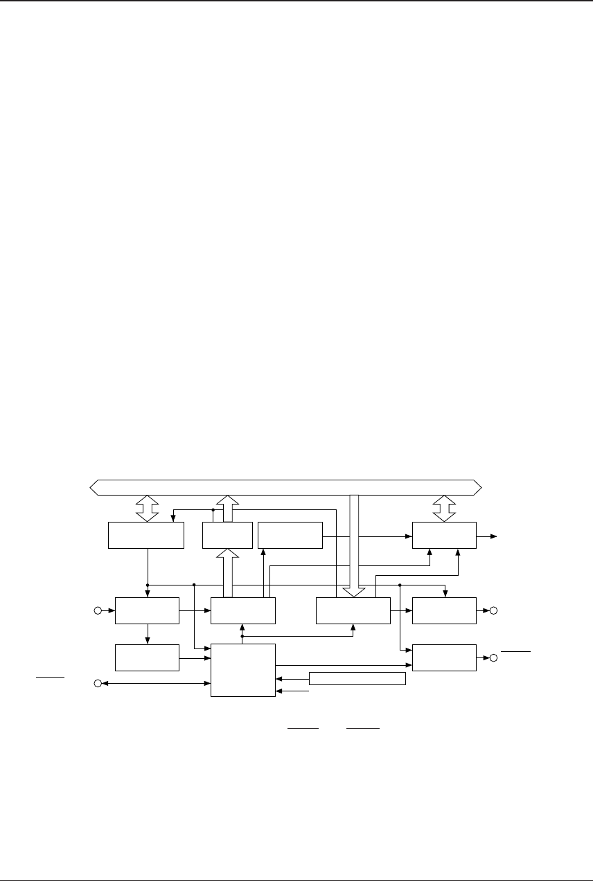
Figure 4.11.1.1 shows the configuration of the serial interface (1). The serial interface (2) has the same
configuration except for the terminals.
f
OSC3
Data bus
SOUT(P11)
Serial I/O control
& status register
Received
data buffer
Interrupt
control circuit
Serial input
control circuit
Received data
shift register
Transmitting data
shift register
Serial output
control circuit
SIN(P10)
Clock
control circuit
READY output
control circuit
SCLK(P12)
Error detection
circuit
SRDY(P13)
Start bit
detection circuit
Programmable timer 1 underflow signal
Interrupt
request
OSC3 oscillation circuit
Fig. 4.11.1.1 Configuration of serial interface
Serial interface input/output terminals, SIN, SOUT, SCLK and SRDY are shared with the I/O ports P10–
P13. In order to utilize these terminals for the serial interface input/output terminals, proper settings have
to be made with registers ESIF, SMD0 and SMD1. (At initial reset, these terminals are set as I/O port
terminals.)
The direction of I/O port terminals set for serial interface input/output terminals are determined by the
signal and transfer mode for each terminal. Furthermore, the settings for the corresponding I/O control
registers for the I/O ports become invalid.