


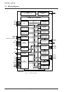

10 EPSON S1C63558 TECHNICAL MANUAL
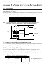
CHAPTER 2: POWER SUPPLY AND INITIAL RESET
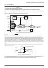
2.2.2 Simultaneous low input to terminals K00–K03
Another way of executing initial reset externally is to input a low signal simultaneously to the input ports
(K00–K03) selected with the mask option.
Since this initial reset passes through the noise reject circuit, maintain the specified input port terminals at
low level for at least 1.5 msec (when the oscillation frequency f
OSC1 is 32.768 kHz) during normal opera-
tion. The noise reject circuit does not operate immediately after turning the power on until the oscillation
circuit starts oscillating. Therefore, maintain the specified input port terminals at low level for at least 1.5
msec (when the oscillation frequency f
OSC1 is 32.768 kHz) after oscillation starts.
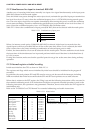
Table 2.2.2.1 shows the combinations of input ports (K00–K03) that can be selected with the mask option.
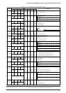
Table 2.2.2.1 Combinations of input ports
Not use
K00∗K01∗K02∗K03
K00∗K01∗K02
K00∗K01
1
2
3
4
When, for instance, mask option 2 (K00∗K01∗K02∗K03) is selected, initial reset is executed when the
signals input to the four ports K00–K03 are all low at the same time. When 3 or 4 is selected, the initial
reset is done when a key entry including a combination of selected input ports is made.
Further, the time authorize circuit can be selected with the mask option. The time authorize circuit checks
the input time of the simultaneous low input and performs initial reset if that time is the defined time (1
to 2 sec) or more.
If using this function, make sure that the specified ports do not go low at the same time during ordinary
operation.
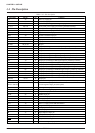
2.2.3 Internal register at initial resetting
Initial reset initializes the CPU as shown in Table 2.2.3.1.
The registers and flags which are not initialized by initial reset should be initialized in the program if
necessary.
In particular, the stack pointers SP1 and SP2 must be set as a pair because all the interrupts including
NMI are masked after initial reset until both the SP1 and SP2 stack pointers are set with software.
When data is written to the EXT register, the E flag is set and the following instruction will be executed in
the extended addressing mode. If an instruction which does not permit extended operation is used as the
following instruction, the operation is not guaranteed. Therefore, do not write data to the EXT register for
initialization only.
Refer to the "S1C63000 Core CPU Manual" for extended addressing and usable instructions.
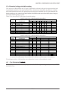
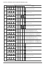
Table 2.2.3.1 Initial values
Name
Data register A
Data register B
Extension register EXT
Index register X
Index register Y
Program counter
Stack pointer SP1
Stack pointer SP2
Zero flag
Carry flag
Interrupt flag
Extension flag
Queue register
CPU core
Symbol
A
B
EXT
X
Y
PC
SP1
SP2
Z
C
I
E
Q
Number of bits
4
4
8
16
16
16
8
8
1
1
1
1
16
Setting value
Undefined
Undefined
Undefined
Undefined
Undefined
0110H
Undefined
Undefined
Undefined
Undefined
0
0
Undefined
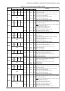
Name
RAM
Display memory
Other pheripheral circuits
Peripheral circuits
Number of bits
4
4
–
Setting value
Undefined
Undefined
∗
∗ See Section 4.1, "Memory Map".