


52 EPSON S1C63558 TECHNICAL MANUAL
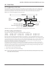
CHAPTER 4: PERIPHERAL CIRCUITS AND OPERATION (LCD Driver)
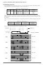
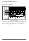
COM0
COM1
COM2
COM3
COM4
COM5
COM6
COM7
COM0
COM1
COM2
COM3
COM4
COM5
COM6
COM7
Unused
SEG0
■ D0
■ D1
■ D2
■ D3
■ D0
■ D1
■ D2
■ D3
■ D0
■ D1
■ D2
■ D3
■ D0
■ D1
■ D2
■ D3
■ D0
F000H
LPAGE
=0
LPAGE
=1
F001H
F100H
F101H
F200H
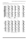
SEG1
■ D0
■ D1
■ D2
■ D3
■ D0
■ D1
■ D2
■ D3
■ D0
■ D1
■ D2
■ D3
■ D0
■ D1
■ D2
■ D3
■ D0
F002H
F003H
F102H
F103H
F202H
SEG2
■ D0
■ D1
■ D2
■ D3
■ D0
■ D1
■ D2
■ D3
■ D0
■ D1
■ D2
■ D3
■ D0
■ D1
■ D2
■ D3
■ D0
F004H
F005H
F104H
F105H
F204H
SEG3
■ D0
■ D1
■ D2
■ D3
■ D0
■ D1
■ D2
■ D3
■ D0
■ D1
■ D2
■ D3
■ D0
■ D1
■ D2
■ D3
■ D0
F006H
F007H
F106H
F107H
F206H
. . . . .
. . . . .
. . . . .
. . . . .
. . . . .
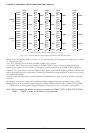
SEG47
■ D0
■ D1
■ D2
■ D3
■ D0
■ D1
■ D2
■ D3
■ D0
■ D1
■ D2
■ D3
■ D0
■ D1
■ D2
■ D3
■ D0
F05EH
F05FH
F15EH
F15FH
F25EH
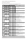
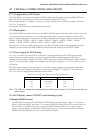
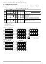
(c) When 1/8 duty (48
×
8 mask option) is selected
Fig. 4.7.5.1 Correspondence between display memory and LCD dot matrix
When a bit in the display memory is set to "1", the corresponding LCD dot goes ON, and when it is set to
"0", the dot goes OFF.
At 1/17 (1/16) duty drive, all data of COM0–COM16 (15) is output.
At 1/8 duty drive, data only corresponding to COM0–COM7 is output. However, since the display
memory has capacity for two screens, it is designed so that the memory for COM8–COM15 shown in
Figure 4.7.5.1 (a) can also be used as COM0–COM15. Select either F000H–F05FH or F100H–F15FH for the
area to be displayed (to be output from COM0–COM7 terminals) using the LPAGE register. It can switch
the screen in an instant.
At initial reset, the data memory content becomes undefined hence, there is need to initialize using the
software.
The display memory has read/write capability, and the addresses that have not been used for LCD
display can be used as general purpose registers. F050H–F05FH, F150H–F15FH, F250H, F252H, F254H,
· · ·, F25EH can be used as general purpose registers except when 48 × 8 is selected by mask option.
Note: When a program that access no memory mounted area (F060H–F0FFH, F160H–F1FFH, F201H,
F203H, · · ·, F25FH) is made, the operation is not guaranteed.