S1C63558 TECHNICAL MANUAL EPSON 83
CHAPTER 4: PERIPHERAL CIRCUITS AND OPERATION (Serial Interface)
(4) Clock source selection
In the master mode, select the synchronous clock source by writing data to the two bits of the
clock source selection registers SCS0 and SCS1. (See Table 4.11.4.1.)
This selection is not necessary in the slave mode.
The parity enable register EPR is also assigned to this address, however, since parity is not neces-
sary in the clock synchronous mode, parity check will not take place regardless of how they are
set.
(5) Clock source control
When the master mode is selected and programmable timer for the clock source is selected, set
transfer rate on the programmable timer side. (See "4.10 Programmable Timer".)
When the divided signal of OSC3 oscillation circuit is selected for the clock source, be sure that the
OSC3 oscillation circuit is turned ON prior to commencing data transfer. (See "4.3 Oscillation
Circuit".)
Note that the frequency of the serial interface clock is limited to a maximum of 1 MHz.
Data transmit procedure
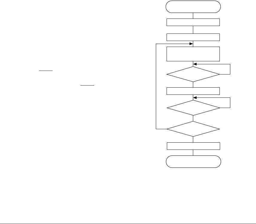
The control procedure and operation during transmitting is as follows.
(1) Write "0" in the transmit enable register TXEN and the receive enable register RXEN to reset the
serial interface.
(2) Write "1" in the transmit enable register TXEN to set into the transmitting enable status.
(3) Write the transmitting data into TRXD0–TRXD7.
(4) In case of the master mode, confirm the receive
ready status on the slave side (external serial input/
output device), if necessary. Wait until it reaches the
receive ready status.
(5) Write "1" in the transmit control bit TXTRG and
start transmitting.
In the master mode, this control causes the synchro-
nous clock to change to enable and to be provided
to the shift register for transmitting and output
from the SCLK terminal.
In the slave mode, it waits for the synchronous
clock to be input from the SCLK terminal.
The transmitting data of the shift register shifts one
bit at a time at each falling edge of the synchronous
clock and is output from the SOUT terminal. When
the final bit (MSB) is output, the SOUT terminal is
maintained at that level, until the next transmitting
begins.
The transmitting complete interrupt factor flag
ISTR is set to "1" at the point where the data
transmitting of the shift register is completed.
When interrupt has been enabled, a transmitting
complete interrupt is generated at this point.
Set the following transmitting data using this
interrupt.
(6) Repeat steps (3) to (5) for the number of bytes of
transmitting data, and then set the transmit disable
status by writing "0" to the transmit enable register
TXEN, when the transmitting is completed.
Data transmitting
End
TXEN ← 0, RXEN ← 0
No
Yes
Transmit complete ?
Set transmitting data
to TRXD0–TRXD7
No
Yes
ISTR = 1 ?
TXEN ← 0
TXTRG ← 1
TXEN ← 1
No
Yes
Receiver ready ?
In case of master mode
Fig. 4.11.6.2 Transmit procedure in clock
synchronous mode


