


13
82575 Ethernet Controller Design Guide
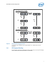
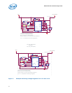
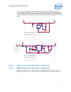
2. A particular address range of the IOADDR register defined by the IO Base Address
Register (PCIe Control Register at offset 18h or 20h).
3. The Expansion ROM Base Address Register (PCIe Control Register at offset 30h).
The 82575 controls accesses to the Flash when it decodes a valid access.
Note: Flash read accesses must always be assembled by the 82575 whenever the access is
greater than a byte-wide access.
Note: Byte reads or writes to the Flash take on the order of 2us. The device will continue to
issue retry accesses during this time.
Note: The 82575 Ethernet Controller supports only byte writes to the Flash.
Another way for SW to access the Flash is directly using the Flash's 4-wire interface
through the Flash Access Register (FLA). It can use this for reads, writes, or other Flash
operations (accessing the Flash status register, erase…).
To directly access the Flash, software should follow these steps:
1. Write a 1 to the Flash Request bit (FLA.FL_REQ)
2. Read the Flash Grant bit (FLA.FL_GNT) until it becomes 1. It will remain 0 as long
as there are other accesses to the Flash.
3. Write or read the Flash using the direct access to the 4-wire interface as defined in
the Flash Access Register (FLA). The exact protocol used depends on the Flash
placed on the board and can be found in the appropriate datasheet.
4. Write a 0 to the Flash Request bit (FLA.FL_REQ).
3.2.4.1 Flash Write Control
The Flash is write controlled by the FWE bits in the EEPROM/FLASH Control and Data
Register (EEC). Note that attempts to write to the Flash device when writes are
disabled (FWE10) should not be attempted. Behavior after such an operation is
undefined, and may result in component and/or system hangs.
After sending one byte write to the flash, the software can check if it can send the next
byte to write (check if the write process in the Flash had finished) by reading the Flash
Access Register. If bit (FLA.FL_BUSY) in this register is set, the current write did not
finish. If bit (FLA.FL_BUSY) is clear, then the software can continue and write the next
byte to the Flash.
3.2.4.2 Flash Erase Control
When software wants to erase the Flash, it should set bit FLA.FL_ER in the Flash Access
Register to one (Flash erase and set bits EEC.FWE in the EEPROM/Flash Control
Register to zero).
The hardware will get this command and send the erase command to the Flash. The
erase process will finish by itself. Software should wait for the end of the erase process
before any further access to the flash. This can be checked by using the Flash Write
control mechanism described earlier.
The op-code used for erase operation is defined in the FLASHOP register.