


82575 Ethernet Controller Design Guide
28
Note that if the device is configured to provide a 50MHz NC-SI clock (via the NC-SI
Output Clock EEPROM bit), then the NC-SI clock must be provided in Device Disable
mode as well the device should not be disabled.
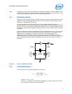
Device Disable is initiated by asserting the asynchronous DEV_OFF_N pin. The
DEV_OFF_N pin has an internal pull-up resistor, so that it can be left not connected to
enable device operation.
The EEPROM’s "Device Disable Power Down En" bit enables device disable mode
(hardware default is that the mode is disabled).
While in device disable mode, the PCI Express link is in L3 state. The PHY is in power
down mode. Output buffers are tri-stated.
Assertion or deassertion of PCI Express PE_RST_N does not have any effect while the
device is in device disable mode (that is, the device stays in the respective mode as
long as DEV_OFF_N is asserted). However, the device may momentarily exit the device
disable mode from the time PCI Express PE_RST_N is de-asserted again and until the
EEPROM is read.
During power-up, the DEV_OFF_N pin is ignored until the EEPROM is read. From that
point, the device may enter Device Disable if DEV_OFF_N is asserted.
Note: The DEV_OFF_N pin should maintain its state during system reset and system sleep
states. It should also insure the proper default value on system power-up. For example,
one could use a GPIO pin that defaults to '1' (enable) and is on system suspend power
(i.e., it maintains state in S0-S5 ACPI states).
3.8.1 BIOS handling of Device Disable
Assume that in the following power up sequence the DEV_OFF_N signal is driven high
(or it is already disabled)
1. The PCIe is established following the GIO_PWR_GOOD
2. BIOS recognizes that the whole Device should be disabled
3. The BIOS drive the DEV_OFF_N signal to the low level.
4. As a result, the device samples the DEV_OFF_N signals and enters either the
device disable mode.
5. The BIOS could put the Link in the Electrical IDLE state (at the other end of the PCI
Express link) by clearing the LINK Disable bit in the Link Control Register.
6. BIOS may start with the Device enumeration procedure (the whole Device
functions are invisible)
7. Proceed with Nominal operation
8. Re-enable could be done by driving hi the DEV_OFF_N signal, followed later by bus
enumeration.
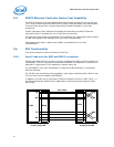
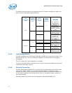
3.9 Software-Definable Pins (SDPs)
The 82575 has four software-defined pins (SDP) per port that can be used for
miscellaneous hardware or software-controllable purposes. These pins and their
function are bound to a specific LAN device (eight SDPs may not be associated with a
single LAN device, for example). These pins can each be individually configured to act
as either input or output pins. The default direction of each of the four pins is
configurable via EEPROM, as well as the default value of any pins configured as
outputs.