


43
82575 Ethernet Controller Design Guide
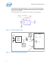
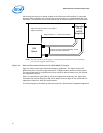
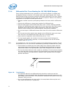
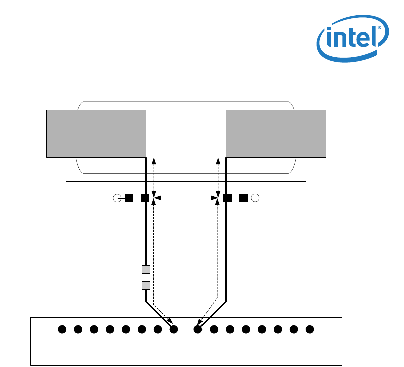
Figure 15. Recommended Crystal Placement and Layout
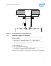
7.1.3 Board Stack Up Recommendations
Printed circuit boards for these designs typically have six, eight, or more layers.
Although, the 82575 does not dictate the stackup, here is an example of a typical six-
layer board stackup:
• Layer 1 is a signal layer. It can contain the differential analog pairs from the
Ethernet device to the magnetics module, or to an optical transceiver.
• Layer 2 is a signal ground layer. Chassis ground may also be fabricated in Layer 2
under the connector side of the magnetics module.
• Layer 3 is used for power planes.
• Layer 4 is a signal layer.
• Layer 5 is an additional ground layer.
• Layer 6 is a signal layer. For 1000 BASE-T (copper) Gigabit designs, it is common to
route two of the differential pairs (per port) on this layer.
This board stack up configuration can be adjusted to conform to your company's design
rules
Crystal Pad Crystal Pad
Ethernet Controller
Xtal1Xtal2
“C”
27pF
0402
27pF
0402
30-ohm
0402
Crystal
“B” “B”
“A”
90 mils
90 mils
Capacitor Capacitor
Resistor
Less than 660 mils