


82575 Ethernet Controller Design Guide
42
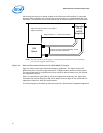
7.1.2 Crystals and Oscillators
Clock sources should not be placed near I/O ports or board edges. Radiation from
these devices may be coupled into the I/O ports and radiate beyond the system
chassis. Crystals should also be kept away from the Ethernet magnetics module to
prevent interference.
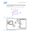
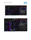
7.1.2.1 Crystal layout considerations
Note: Failure to follow these guidelines could result in the 25 MHz clock failing to start.
When designing the layout for the crystal circuit, the following rules must be used:
• Place load capacitors as close as possible (within design-for-manufacturability
rules) to the crystal solder pads. They should be no more than 90 mils away from
crystal pads.
• The two load capacitors, crystal component, the Ethernet controller device, and the
crystal circuit traces must all be located on the same side of the circuit board
(maximum of one via-to-ground load capacitor on each Xtal trace).
• Use 27 pF (5% tolerance) 0402 load capacitors.
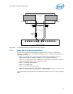
• Place load capacitor solder pad directly in line with circuit trace (see Figure 15,
point A).
• Place a 30-ohm (5% tolerance) 0402 series resistor on Xtal2 (see Figure 15, point
C). The location of the resistor along the Xtal2 trace is flexible, as long as it is
between the load capacitor and the controller.
• Use 50-ohm impedance single-ended microstrip traces for the crystal circuit.
• Route traces so that electro-magnetic fields from Xtal2 do not couple onto Xtal1.
No differential traces.
• Route Xtal1 and Xtal2 traces to nearest inside corners of crystal pad (see Figure 15,
point B).
• Ensure that the traces from Xtal1 and Xtal2 are symmetrically routed and that their
lengths are matched.
• The total trace length of Xtal1 or Xtal2 should be less than 750 mils.