


3
82575 Ethernet Controller Design Guide
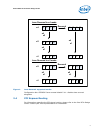
2.0 PCI Express Port Connection to the Device
PCI Express (PCIe*) is a dual simplex point-to-point serial differential low-voltage
interconnect. The signaling bit rate is 2.5 Gbps per lane per direction. Each port
consists of a group of transmitters and receivers located on the same chip. Each lane
consists of a transmitter and a receiver pair. A link between the ports of two devices is
a collection of lanes. The device supports up to four lanes on the PCIe interface.
Each signal is 8b/10b encoded with an embedded clock.
The PCI Express topology consists of a transmitter (Tx) located on one device
connected through a differential pair connected to the receiver (Rx) on a second
device. The controller may be located on the motherboard or on an add-in card using a
connector specified by PCI Express.
The lane is AC-coupled between its corresponding transmitter and receiver. The AC-
coupling capacitor is located on the board close to transmitter side. Each end of the link
is terminated on the die into nominal 100 Ω differential DC impedance. Board
termination is not required.
For more information on PCI Express, refer to the PCI Express* Base Specification,
Revision 1.1 and PCI Express* Card Electromechanical Specification, Revision 1.1RD.
For information about PCIe power management with the 82575, refer to section 3.4 in
this document.
2.1 PCI Express Reference Clock
The device uses a 100 MHz differential reference clock, denoted PE_CLK_P and
PE_CLK_N. This signal is typically generated on the system board and routed to the PCI
Express port. For add-in cards, the clock will be furnished at the PCI Express connector.
The frequency tolerance for the PCI Express reference clock is +/- 300 ppm.
2.2 Other PCI Express Signals
The device also implements other signals required by the PCI Express specification. The
Ethernet controller signals power management events to the system using the
PE_WAKE# signal, which operates very similarly to the familiar PCI PME# signal.
Finally, there is a PE_RST# signal which serves as the familiar reset function for the
controller.
2.3 Physical Layer Features
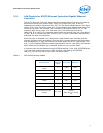
2.3.1 Link Width Configuration
The device supports a maximum link width of x4, x2, or x1 as determined by the
EEPROM Lane_Width field in PCIe init configuration.
The max link width is loaded into the Maximum Link Width field of the PCIe capability
Register (LCAP[11:6]). The 82575 Ethernet Controller default is x4 link.
During link configuration, the platform and the 82575 Ethernet Controller negotiate on
a common link width. The link width must be one of the supported PCIe link widths (1x,
2x, 4x), such that:
• If Maximum Link Width = x4, then the 82575 Ethernet Controller negotiates to
either x4, x2 or x1