


35
82575 Ethernet Controller Design Guide
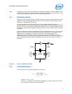
Even with a perfect support circuit, most crystals will oscillate slightly higher or slightly
lower than the exact center of the target frequency. Therefore, frequency
measurements (which determine the correct value for C1 and C2) should be performed
with an ideal reference crystal. When the capacitive load is exactly equal to the
crystal’s load rating, an ideal reference crystal will be perfectly centered at the desired
target frequency.
5.11.1 Reference Crystal Selection
There are several methods available for choosing the appropriate reference crystal:
• If a Saunders and Associates (S&A) crystal network analyzer is available, then
discrete crystal components can be tested until one is found with zero or nearly
zero ppm deviation (with the appropriate capacitive load). A crystal with zero or
near zero ppm deviation will be a good reference crystal to use in subsequent
frequency tests to determine the best values for C1 and C2.
• If a crystal analyzer is not available, then the selection of a reference crystal can be
done by measuring a statistically valid sample population of crystals, which has
units from multiple lots and approved vendors. The crystal, which has an oscillation
frequency closest to the center of the distribution, should be the reference crystal
used during testing to determine the best values for C1 and C2.
• It may also be possible to ask the approved crystal vendors or manufacturers to
provide a reference crystal with zero or nearly zero deviation from the specified
frequency when it has the specified CLoad capacitance.
When choosing a crystal, customers must keep in mind that to comply with IEEE
specifications for 10/100 and 10/100/1000Base-T Ethernet LAN, the transmitter
reference frequency must be precise within ±50 ppm. Intel® recommends customers to
use a transmitter reference frequency that is accurate to within ±30 ppm to account for
variations in crystal accuracy due to crystal manufacturing tolerance..
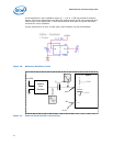
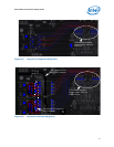
5.11.2 Circuit Board
Since the dielectric layers of the circuit board are allowed some reasonable variation in
thickness, the stray capacitance from the printed board (to the crystal circuit) will also
vary. If the thickness tolerance for the outer layers of dielectric are controlled within
±17 percent of nominal, then the circuit board should not cause more than ±2 pF
variation to the stray capacitance at the crystal. When tuning crystal frequency, it is
recommended that at least three circuit boards are tested for frequency. These boards
should be from different production lots of bare circuit boards.
Alternatively, a larger sample population of circuit boards can be used. A larger
population will increase the probability of obtaining the full range of possible variations
in dielectric thickness and the full range of variation in stray capacitance.
Next, the exact same crystal and discrete load capacitors (C1 and C2) must be soldered
onto each board, and the LAN reference frequency should be measured on each circuit
board.
The circuit board, which has a LAN reference frequency closest to the center of the
frequency distribution, should be used while performing the frequency measurements
to select the appropriate value for C1 and C2.
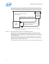
5.11.3 Temperature Changes
Temperature changes can cause the crystal frequency to shift. Therefore, frequency
measurements should be done in the final system chassis across the system’s rated
operating temperature range.