


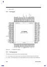

Major Chips Description 2-63
Table 2-7 CL-PD6832 Pin Descriptions
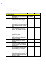
Pin Name Description Pin Number I/O Power
PERR#
Parity Error: The CL-PD6832 drives this
output active (low) if it detects a data parity
error during a write phase.
33 I/O 4
SERR#
System Error: This output is pulsed by the CL-
PD6832 to indicate an address parity error.
34 O-
OD
4
PAR
Parity: This pin is sampled the clock cycle
after completion of each corresponding
address or write data phase. For read
operations this pin is driven from the cycle after
TRDY# is asserted until the cycle after
completion of each data phase. It ensures even
parity across AD[31:0] and C/BE[3:0]#.
35 I/O 4
PCI_CLK
PCI Clock: This input provides timing for all
transactions on the PCI bus to and from the
CL-PD6832. All PCI bus interface signals
described in this table, except RST#, INTA#,
INTB#, INTC#, and INTD#, are sampled on the
rising edge of PCI_CLK; and all CL-PD6832
PCI bus interface timing parameters are
defined with respect to this edge. This input
can be operated at frequencies from 0 to 33
MHz.
1 I
RST#
Device Reset: This input is used to initialize all
registers and internal logic to their reset states
and place most CL-PD6832 pins in a high-
impedance state.
207 I
INTA#/
IRQ9
PCI Bus Interrupt A / ISA Interrupt Request
9: This output indicates a programmable
interrupt request generated from any of a
number of card actions. Although there is no
specific mapping requirement for connecting
interrupt lines from the CL-PD6832 to the
system, a common use is to connect this pin to
the PCI bus INTA# interrupt line and using PCI
Interrupt Signaling mode. In External-Hardware
Interrupt Signaling mode, this pin indicates
interrupt request IRQ9.
203 O-TS 4
Rl_OUT*/
INTB#/
IRQ10
Ring Indicate Output / PCI Bus Interrupt B /
ISA Interrupt Request 10: In PCI Interrupt
Signaling mode, this output can be used as an
interrupt output connected to the PCI bus
INTB# interrupt line. If Misc Control 2 register
bit 7 is ‘1’, as a ring indicate output from a
socket’s BVD1/-STSCHG/-RI input. In External-
Hardware Interrupt Signaling mode, this pin
indicates interrupt request IRQ10.
204 O-TS 4