


2-22 Service Guide
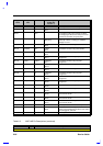
Table 2-2 82371AB Pin Descriptions
Name Type Description
SDDREQ I
SECONDARY DISK DMA REQUEST. This input signal is directly driven from
the IDE device DMARQ signal. It is asserted by the IDE device to request a data
transfer, and used in conjunction with the PCI bus master IDE function. It is not
associated with any AT compatible DMA channel. If the IDE signals are
configured for Primary and Secondary, this signal is connected to the
corresponding signal on the Secondary IDE connector. If the IDE signals are
configured for Primary Master and Primary Slave, these signals are used for the
Primary Slave connector.
SDIOR# O
SECONDARY DISK IO READ. In normal IDE mode, this is the command to the
IDE device that it may drive data onto the SDD[15:0] lines. Data is latched by the
PIIX4 on the negation edge of SDIOR#. The IDE device is selected either by the
ATA register file chip selects (SDCS1#, SDCS3#) and the SDA[2:0] lines, or the
IDE DMA slave arbitration signals (SDDACK#). In an Ultra DMA/33 read cycle,
this signal is used as DMARDY# which is negated by the PIIX4 to pause Ultra
DMA/33 transfers. In an Ultra DMA/33 write cycle, this signal is used as the
STROBE signal, with the drive latching data on rising and falling edges of
STROBE. If the IDE signals are configured for Primary and Secondary, this
signal is connected to the corresponding signal on the Secondary IDE connector.
If the IDE signals are configured for Primary Master and Primary Slave, these
signals are used for the Primary Slave connector.
During Reset: High After Reset: High During POS: High
SDIOW# O
SECONDARY DISK IO WRITE. In normal IDE mode, this is the command to the
IDE device that it may latch data from the SDD[15:0] lines. Data is latched by
the IDE device on the negation edge of SDIOW#. The IDE device is selected
either by the ATA register file chip selects (SDCS1#, SDCS3#) and the SDA[2:0]
lines, or the IDE DMA slave arbitration signals (SDDACK#). In read and write
cycles this signal is used as the STOP signal, which is used to terminate an
Ultra DMA/33 transaction. If the IDE signals are configured for Primary and
Secondary, this signal is connected to the corresponding signal on the
Secondary IDE connector. If the IDE signals are configured for Primary Master
and Primary Slave, these signals are used for the Primary Slave connector.
During Reset: High After Reset: High During POS: High
SIORDY I
SECONDARY IO CHANNEL READY. In normal IDE mode, this input signal is
directly driven by the corresponding IDE device IORDY signal. In an Ultra
DMA/33 read cycle, this signal is used as STROBE, with the PIIX4 latching data
on rising and falling edges of STROBE. In an Ultra DMA write cycle, this signal
is used as the DMARDY# signal which is negated by the drive to pause Ultra
DMA/33 transfers. If the IDE signals are configured for Primary and Secondary,
this signal is connected to the corresponding signal on the Secondary IDE
connector. If the IDE signals are configured for Primary Master and Primary
Slave, these signals are used for the Primary Slave connector. This is a Schmitt
triggered input.
Note: After reset, all undefined signals on the primary channel will default to the same values as the
undefined signals on the secondary channel.
UNIVERSAL SERIAL BUS SIGNALS
OC[1:0]# I
OVER CURRENT DETECT. These signals are used to monitor the status of the
USB power supply lines. The corresponding USB port is disabled when its over
current signal is asserted.