


Major Chips Description 2-31
2.3.3 Pin Descriptions
Conventions used in the pin description types:
I Input into NM2160
O Output from NM2160
I/O Input and Output to/from NM2160
T/S Tri-state during un-driven state
S/T/S Before becoming tri-state the pin will be driven inactive
O/D Open-drain type output
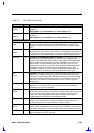
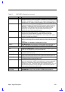
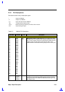
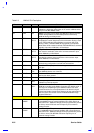
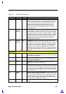
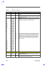
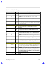
Table 2-3 NM2160 Pin Descriptions
Pin name Number I/O Description
PCI Interface
61
60
58
56
55
54
53
52
50
49
48
47
46
45
43
41
39
38
37
36
35
34
33
32
30
28
26
24
22
21
20
19
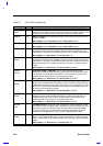
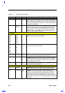
AD31
AD30
AD29
AD28
AD27
AD26
AD25
AD24
AD23
AD22
AD21
AD20
AD19
AD18
AD17
AD16
AD15
AD14
AD13
AD12
AD11
AD10
AD9
AD8
AD7
AD6
AD5
AD4
AD3
AD2
AD1
AD0
I/O
T/S
Multiplexed Address and Data 31:0 These multiplexed and bi-
directional pins are used to transfer address and data on the PCI
bus. The bus master will drive the 32-bit physical address during
address phase and data during data phase for write cycles.
NM2160 will drive the data bus during data phase for read cycles
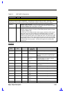
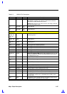
63
51
40
31
C/BE3#
C/BE2#
C/BE1#
C/BE0#
I/O
Multiplexed Command and Byte Enable These multiplexed pins
provide the command during address phase and byte enable(s)
during data phase to the NM2160. NM2160 drives this pin in the
Bus Master mode