


Major Chips Description 2-19
Table 2-2 82371AB Pin Descriptions
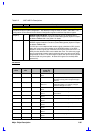
Name Type Description
PCICLK I
FREE-RUNNING PCI CLOCK. A clock signal running at 30 or 33 MHz, PCICLK
provides timing for all transactions on the PCI Bus. All other PCI signals are
sampled on the rising edge of PCICLK, and all timing parameters are defined
with respect to this edge. Because many of the circuits in PIIX4 run off the PCI
clock, this signal MUST be kept active, even if the PCI bus clock is not active.
OSC I
14.31818-MHZ CLOCK. Clock signal used by the internal 8254 timer. This clock
signal may be stopped during suspend modes.
RTCX1,
RTCX2
I/O
RTC CRYSTAL INPUTS: These connected directly to a 32.768-kHz crystal.
External capacitors are required. These clock inputs are required even if the
internal RTC is not being used.
SUSCLK O
SUSPEND CLOCK. 32.768-kHz output clock provided to the Host-to-PCI bridge
used for maintenance of DRAM refresh. This signal is stopped during Suspend-
to-Disk and Soft Off modes. For values During Reset, After Reset, and During
POS, see the Suspend/Resume and Resume Control Signaling section.
SYSCLK O
ISA SYSTEM CLOCK. SYSCLK is the reference clock for the ISA bus. It drives
the ISA bus directly. The SYSCLK is generated by dividing PCICLK by 4. The
SYSCLK frequencies supported are 7.5 MHz and 8.33 MHz. For PCI accesses to
the ISA bus, SYSCLK may be stretched low to synchronize BALE falling to the
rising edge of SYSCLK.
During Reset: Running After Reset: Running During POS: Low
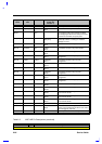
IDE SIGNALS
PDA[2:0] O
PRIMARY DISK ADDRESS[2:0]. These signals indicate which byte in either the
ATA command block or control block is being addressed. If the IDE signals are
configured for Primary and Secondary, these signals are connected to the
corresponding signals on the Primary IDE connector. If the IDE signals are
configured for Primary 0 and Primary 1, these signals are used for the Primary 0
connector.
During Reset: High-Z After Reset: Undefined During POS: PDA
PDCS1# O
PRIMARY DISK CHIP SELECT FOR 1F0H-1F7H RANGE. For ATA command
register block. If the IDE signals are configured for Primary and Secondary, this
output signal is connected to the corresponding signal on the Primary IDE
connector. If the IDE signals are configured for Primary Master and Primary
Slave, this signal is used for the Primary Master connector.
During Reset: High After Reset: High During POS: High
PDCS3# O
PRIMARY DISK CHIP SELECT FOR 3F0-3F7 RANGE. For ATA control register
block. If the IDE signals are configured for Primary and Secondary, this output
signal is connected to the corresponding signal on the Primary IDE connector. If
the IDE signals are configured for Primary Master and Primary Slave, this signal
is used for the Primary Master connector.
During Reset: High After Reset: High During POS: High
PDD[15:0] I/O
PRIMARY DISK DATA[15:0]. These signals are used to transfer data to or from
the IDE device. If the IDE signals are configured for Primary and Secondary,
these signals are connected to the corresponding signals on the Primary IDE
connector. If the IDE signals are configured for Primary Master and Primary
Slave, this signal is used for the Primary Master connector.
During Reset: High-Z After Reset: Undefined During POS: PDD