


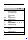
Major Chips Description 2-65
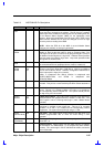
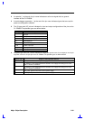
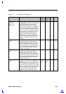
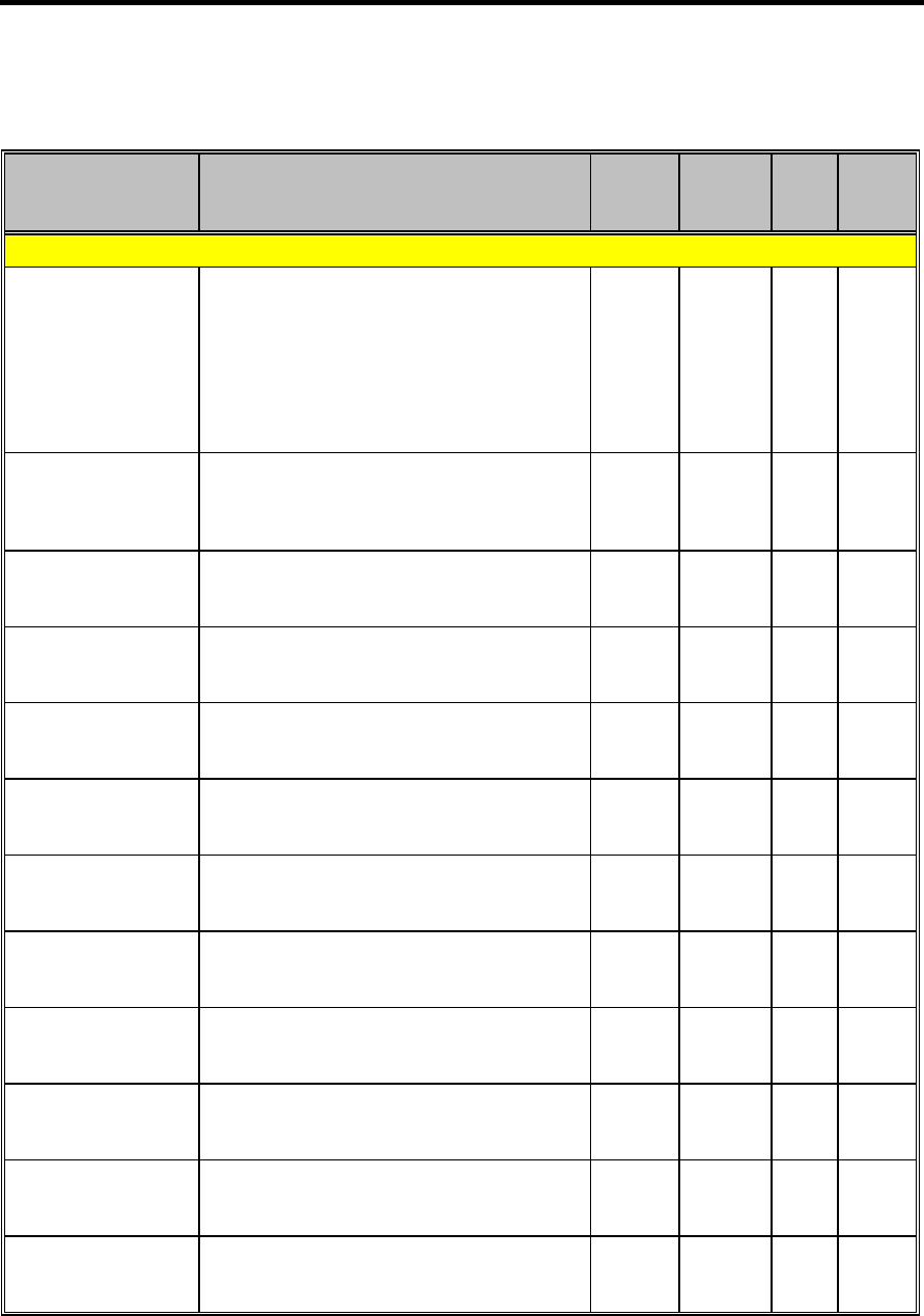
Table 2-7 CL-PD6832 Pin Descriptions
Pin Name Description Pin No.
(socke
t A)
Pin No.
(socket
B)
I/O Power
Socket Interface Pins
-REG/
CC/BE3#
Register Access: In Memory Card
Interface mode, this output chooses
between attribute and common memory. In
l/O Card Interface mode, this signal is
active (low) for non DMA transfers and high
for DMA transfers. In ATA mode this
signal is always high. In CardBus mode,
this pin is the command and byte enables.
112 188 I/O 2 or 3
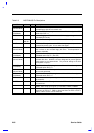
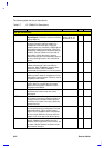
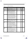
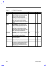
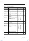
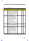
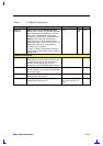
A[25:24]/
CAD[19,17]
PCMCIA socket address 25:24 outputs.
In CardBus mode, these pins are the
CardBus address/data bits 19 and 17,
respectively.
102, 99 176,
174
I/O 2 or 3
A23/
CFRAME#
PCMCIA socket address 23 output. In
CardBus mode, this pin is the Cardbus
FRAME# signal.
96 172 I/O 2 or 3
A22/
CTRDY#
PCMCIA socket address 22 output. In
CardBus mode, this pin is the Cardbus
TRDY# signal.
94 170 I/O 2 or 3
A21/
CDEVSEL#
PCMCIA socket address 21 output. In
CardBus mode, this pin is the Cardbus
DEVSEL# signal.
92 168 I/O 2 or 3
A20/
CSTOP#
PCMCIA socket address 20 output. In
CardBus mode, this pin is the Cardbus
STOP# signal.
90 166 I/O 2 or 3
A19/
CBLOCK#
PCMCIA socket address 19 output. In
CardBus mode, this signal is the CardBus
LOCK# signal used for locked transactions.
88 164 I/O 2 or 3
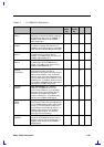
A18/
RFU
PCMCIA socket address 18 output. In
CardBus mode, this pin is reserved for
future use.
85 161 O 2 or 3
A17/
CAD16
PCMCIA socket address 17 output. In
CardBus mode, this pin is the Cardbus
address/data bit 16.
83 158 I/O 2 or 3
A16/
CCLK
PCMCIA socket address 16 output. In
CardBus mode, this pin supplies the clock
to the inserted card.
93 169 O 2 or 3
A15/
CIRDY#
PCMCIA socket address 15 output. In
CardBus mode, this pin is the Cardbus
IRDY# signal.
95 171 I/O 2 or 3
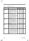
A14/
CPERR#
PCMCIA socket address 14 output. In
CardBus mode, this pin is the Cardbus
PERR# signal.
86 162 I/O 2 or 3