


2-66 Service Guide
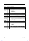
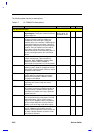
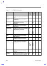
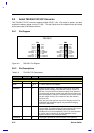
Table 2-7 CL-PD6832 Pin Descriptions
Pin Name Description Pin No.
(socke
t A)
Pin No.
(socket
B)
I/O Power
A13/
CPAR
PCMCIA socket address 13 output. In
CardBus mode, this pin is the Cardbus PAR
signal.
84 159 I/O 2 or 3
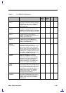
A12/
CC/BE2#
PCMCIA socket address 12 output. In
CardBus mode, this pin is the Cardbus
C/BE2# signal.
97 173 I/O 2 or 3
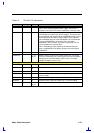
A[11:9]/
CAD[12,9,14]
PCMCIA socket address 11:9 outputs. In
CardBus mode, these pins are the Cardbus
address/data bits 12, 9, and 14,
respectively.
77, 73,
80
153,
149,
155
I/O 2 or 3
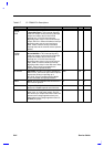
A8/
CC/BE1#
PCMCIA socket address 8 output. In
CardBus mode, this pin is the Cardbus
C/BE1# signal.
82 157 I/O 2 or 3
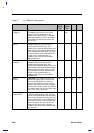
A[7:0]/
CAD[18, 20-26]
PCMCIA socket address 7:0 outputs. In
CardBus mode, these pins are the Cardbus
address/data bits 18 and 20-26,
respectively.
100,
103,
105,
107,
109,
111,
113,
116
175,
178,
181,
183,
185,
187,
189,
191
I/O 2 or 3
D15/
CAD8
PCMCIA socket data I/O bit 15. In
CardBus mode, this pin is the Cardbus
address/data bit 8.
71 148 I/O 2 or 3
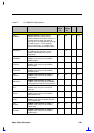
D14/
RFU
PCMCIA socket data I/O bit 14. In
CardBus mode, this pin is reserved for
future use.
69 145 I/O 2 or 3
D[13:3]/
CAD[6,4,2,31, 30,
28, 7, 5, 3, 1, 0]
PCMCIA socket data I/O bits 13:3. In
CardBus mode, this pin is the Cardbus
address/data bit 6 4,2,31,30,28,7,5,3,1, and
0, respectively.
67, 65,
63,
124,
122,
120,
68, 66,
64, 62,
59
142,
140,
138,
199,
197,
195,
144,
141,
139,
137,
135
I/O 2 or 3
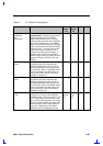
D2/RFU
PCMCIA socket data I/O bit 2. In
CardBus mode, this pin is reserved for
future use.
123 198 I/O 2 or 3
D[1:0]/
CAD[29,27]
PCMCIA socket data I/O bit 1:0. In
CardBus mode, these pins are the Cardbus
address/data bits 29 and 27, respectively.
121,
119
196,
194
I/O 2 or 3