


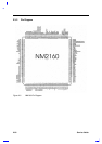
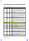

Major Chips Description 2-33
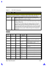
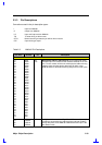
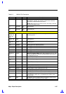
Table 2-3 NM2160 Pin Descriptions
Pin name Number I/O Description
83 XCKEN I
External Clock Enable This pin is used to select between
internally synthesized clocks or externally supplied clocks. A low
level on the pin selects internal mode and a high level selects
external mode. In the external clock mode, the internal clock
synthesizers will be disabled completely. Both PVCLK and
PMCLK pins should be driven with the desired clock rates in
external mode. This pin should be driven all the time during
normal operation
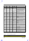
86 PMCLKI/
SRATUS4/
PNLCKI
I/O
T/S
Memory Clock This pin is used for feeding external memory
clock or observing internal memory clock. When in internal clock
mode(XCKEN=0), the internal memory clock can be brought out
using this pin. When in external clock mode (XCKEN=1), PMCLKI
should be driven from an external memory clock source. General
purpose Status bit 4 can be read from register CR27 bit 1(GR17
bit 0 defines the function of this pin). GR17 bit 7 enables the
Modulated Clock Input function(PNLCKI) from the Spread
Spectrum Clock Generator
85 PVCLKI/
STATUS3/
PNLCKO
I/O
T/S
Video Clock This pin is used for feeding external video clock or
observing internal video clock. When in internal clock mode
(XCKEN=0), the internal video clock can be brought out using this
pin. When in external clock mode(XCKEN=1). PVCLKI should be
driven from an external video clock source. General purpose
Status bit 3 can be read from register CR27 bit 2. (GR17 bit 1
defines the function of this pin). GR17 bit 7 enables the Reference
clock output function(PNCLKO) to the Spread Spectrum Clock
Generator
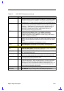
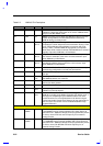
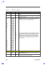
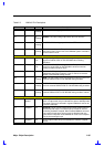
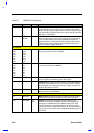
Panel Interface
112 FLM O
First Line Marker This signal indicates start of a frame. For STN
panels this pin is connected to FLM pin. For TFT panels this pin is
connected to the VSYNC pin
113 LP O
Line Pulse This signal indicates start of a line. For STN panels
this pin is connected to the CP1 pin. For TFT panels this pin is
connected to the HSYNC pin
141 SCLK O
Shift Clock This signal is used to drive the panel shift clock.
Some panel manufactures call this CP2
115 SCLKI O
Shift Clocki This signal is used to drive the panel shift clock or as
a General Purpose Output Pin. This clock is used for panels which
use two clocks, one for the upper panel and the other for the lower
panel. This pin is also configured as a General Purpose Output
Pin as defined in register CR2F bits 1&0, to control the IMI chip
for reduced EMI
111 FPHDE/
MOD
O
Panel horizontal Display Enable/MOD This signal indicates the
horizontal display time to the panels. For some panels it is used
to drive the shift clock enable pin. This pin can also be configured
to drive FPHDE for certain types of TFT panels which require
separate horizontal display time indicator. Modulation This signal
is used to drive the panel MOD or AC input
142 FPVCC O
Flat Panel VCC This is used to control the logic power to the
panels