


2-56 Service Guide
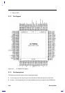
Table 2-6 NS87338VJG Pin Descriptions
Pin No. I/O Description
IRTX 63 O
Infrared Transmit. Infrared serial data output. Software configuration
selects either IrDA or Sharp-IR protocol.
This pin is multiplexed with SOUT2/BOUT/CFG0.
MR 100 I
Master Reset. Active high output that resets the controller to the idle
state and resets all disk interface outputs to their inactive states. The
DOR, DSR, CCR, Mode command, Configure command, and Lock
command parameters are cleared to their default values. The Specify
command parameters are not affected
/MSEN0
/MSEN1
(Normal Mode)
50, 49 I
Media Sense. These pins are Media Sense input pins when bit 0 of
FCR is 0. Each pin has a 10 KΩ internal pull-up resistor. When bit 0
of FCR is 1, these pins are Data Rate output pins and the pull-up
resistors are disabled.
/MSEN0
/MSEN1
(PPM Mode)
86, 84 I
Media Sense. These pins gives additional Media Sense signals for
PPM Mode and PNF = 0.
/MTR0
/MTR1
(Normal Mode)
44, 41 O
FDC Motor Select 0, 1. These are the motor enable lines for drives 0
and 1, and are controlled by bits D7-D4 of the Digital Output register.
They are active low outputs. They are encoded with information to
control four FDDs when bit 4 of the Function Enable Register (FER) is
set. MTR0 exchanges logical motor values with MTR1 when bit 4 of
FCR is set.
/MTR1
(PMM Mode)
82 O
FDC Motor Select 1. This pin offers an additional Motor Select 1
signal in PPM mode when PNF = 0. This pin is the motor enable line
for drive 1 when bit 4 of FCR is 0. It is the motor enable line for drive
0 when bit 4 of FCR 1. This signal is active low
PD 43 O
FDC Power Down. This pin is PD output when bit 4 of PMC is 1. It is
/DR1 when bit 4 of PMC is 0. PD is active high whenever the FDC is
in power-down state, either via bit 6 of the DSR (or bit 3 of FER, or bit
0 of PTR), or via the mode command.
PD0-7 92-89,
87-84
I/O
Parallel Port Data. These bidirectional pins transfer data to and from
the peripheral data bus and the parallel port Data Register. These
pins have high current drive capability.
PE 81 I
Parallel Port Paper End. This input is set high by the printer when it
is out of paper. This pin has a nominal 25 KΩ pull-down resistor
attached to it.
PNF 47 I
Printer Not Floppy. PNF is the Printer Not Floppy pin when bit 2 of
FCR is 1. It selects the device which is connected to the PPM pins. A
parallel printer is connected when PNF = 1 and a floppy disk drive is
connected when PNF = 0. This pin is the DRV2 input pin when bit 2 of
FCR is 0.
/RD 17 I
Read. Active low input to signal a data read by the microprocessor.
/RDATA
(Normal Mode)
33 I
FDD Read Data. This input is the raw serial data read from the floppy
disk drive.
/RDATA
(PPM Mode)
89 I
FDD Read Data. This pin supports an additional Read Data signal in
PPM Mode when PNF = 0.