


Major Chips Description 2-73
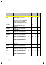
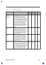
Table 2-8 T62.036.C Pin Descriptions
Pin Name Pin Type Pin No. Description
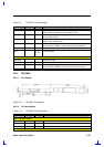
indicate the current drawn from the AC adapter or other power
source such as docking station power supply. This level is 2
Amps per volt nominal. The source impedance is less than 1KΩ.
CHARGSP I 14 Analog input from the system board to limit the total current
consumed by the system from the AC adapter. This signal shall
be compared by the module with the CHARGFB from the system
mother board and the battery charger output current adjusted
until CHARGFB does not exceed CHARGSP. The system board
generates CHARGESP in conjunction with a ID resistor
embedded in the LCD cable. The scale is 2 amps per volt. The
source impedance is less than 2KΩ.
Note: The battery charger output may be reduced below the
level of CHARGESP by the battery charger current limit signal
CHARGECL.
GND GND 15, 16 Ground
CHRGOUT I 17, 18,
19, 20
Battery charger current source output at 3.5A max. The output
current is controlled by two control signals which limit the battery
charging current and AC adapter output current. The output
voltage is limited to 13.2V~13.5V.
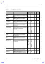
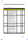
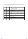
CN2 signals
P12VR O 1, 2 +12V output, 0~0.5A.
GND GND 3, 4, 15,
16
Ground
P3VR O 5, 6, 7, 8 +3.3V output, 0~3A.
BMCVCC O 11, 13 +5V output, 0~0.5A. Used for resuming from suspend-to-
memory mode.
P3VRON O 12 Enables P3VR. Logic level, Active high, +/-luA max loading
P5VRON O 14 Enables PSVR. Logic level, Active high, +/-luA max loading
P5VR O 17, 18,
19, 20
+5V output, 0~2.5A.