


1-24 Service Guide
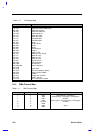
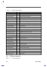
Table 1-13 GPIO Port Definition Map II
GPIO I/O Description
P2.0 I NC
P2.1 O NC
P2.2 (SM5_BAYSW) I Detect FDD/CD bay installed or not
P2.3 O NC
P2.4 O NC
P2.5 O NC
P2.6 O NC
P2.7 O NC
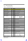
P3.0 (SM5_RXD) I Receiving data from KBC to SMC
P3.1 (SM5_TXD) O Transmitting data from SMC to KBC
P3.2 (SM5_DOCKSW) I Dock switch sense
P3.3 (CF5_DOCKED) I Detect completely docked or not
P3.4 (SM5_LIDSW) I Lid switch sense
P3.5 (SM5_OVTMP#) O CPU or system over temperature
P3.6 O NC
P3.7 (SM5_ON_RES_SW) O ON/RESUME switch for Japan version
P4.0 (SM5_FANON) O Fan control
P4.1 NC
P4.2 (SM5_FLOATREQ#) O Docking float request
P4.3 (SM5_UNDOCK_GNT#) O Undock grant
P4.4 (SM5_ICONT) I Charge current control
P4.5 (SM5_FLAOTGNT#) I Docking float grant
P4.6 (SM5_PWRRDYB) O Power ready, delay about 4ms after power good
P4.7 (SM5_SYSRDY) O NC
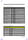
P5.0 (CHARGSP) I Charging set point
P5.1 (SM5_VBAT_MAIN) I Main battery detection
P5.2 (SM5_ACPWRGD) I AC source power good
P5.3 (SM5_NBPWRGD) I 3V, 5V, processor module power good
P5.4 (SM5_ATFINT) I CPU thermal interrupt (panic)
P5.5 (SM5_THERM_SYS) I System thermal input (analog)
P5.6 (SM5_ACIN_AUX) I Aux AC adapter in
P5.7 (SM5_ACIN_MAIN) I Main AC adapter in
PWM1# (SM5_CONT) O LCD contrast
PWM0# (SM5_BRIT) O LCD brightness
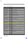
1.6.6 PCI Devices Assignment
Table 1-14 PCI Devices Assignment