


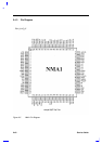

2-36 Service Guide
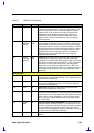
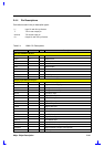
Table 2-3 NM2160 Pin Descriptions
Pin name Number I/O Description
75 Activity I/O
Activity This pin when in input mode and asserted indicates the
system activity. A high on this pin can be used to reset internal
timers. This pin when in output mode is a General Purpose Output
pin as defined by CR2F bits 5&4, which can be used to control the
IMI chip for reduced EMI
82 RTC32K/
Status2
I/O
Real Time Clock 32Khz/Status2 This pin is used to feed 32 kHz
from an external source. It is used to generate the refresh timing
for the internal display memory during Standby and software
Suspend modes. 14 MHz can be used to generate the memory
refresh timing in above modes. / General purpose Status bit 3,
can be read from register CR27 bit 0
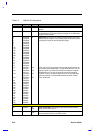
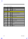
ZV Interface
167
166
165
164
163
162
161
160
UV7
UV6
UV5
UV4
UV3
UV2
UV1
UV0
I
Chrominance Data 7:0 These are the 8-bits of chrominance data
that are input to the ZV port of NM2160
159
158
155
152
151
150
149
148
Y7
Y6
Y5
Y4
Y3
Y2
Y1
Y0
I
Luminance Data 7:0 These are the 8-bits of luminance data that
are input to the ZV port of NM2160
144 HREF I
Horizontal Synchronization Pulse: This input signal provides
the horizontal synchronization pulse to the ZV port
168 PCLK I
Video Clock This signal is used to clock the valid video data and
the HREF signal into the ZV Port. The maximum rate is 16 MHz.
During display time, rising edge of PCLK is used to clock the 16-
bit pixel data into the ZV Port
146 VS I
Vertical SYNC This signal supplies the Vertical synchronization
pulse to the ZV Port of NM2160
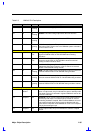
Miscellaneous Pins
87 MTEST# I
Memory test This active low signal is used for internal memory
testing. This should be tied high for normal system operation
145 CLKRUN# I/O
O/D
Clockrun The master device will control this signal to the
NM2160, according to the Mobile computing PCI design guide. If
this signal is sampled high by the NM2160 and the PCI clock
related functions are not completed then it will drive this signal
Low to request the Central Clock Resource for the continuation of
the PCI clock. This function can be Enabled/Disabled through reg.
GR12 bit 5