


2-46 Service Guide
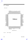
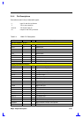
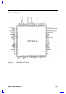
2.5.4 Pin Descriptions
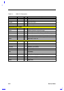
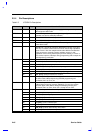
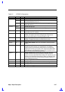
Table 2-5 87C552 Pin Descriptions
Mnemonic Pin No. Type Name And Function
VDD 2 I
Digital Power Supply: +5V power supply pin during normal operation,
idle and power-down mode.
STADC 3 I
Start ADC Operation: Input starting analog to digital conversion (ADC
operation can also be started by software).
PWM0# 4 O
Pulse Width Modulation: Output 0.
PWM1# 5 O
Pulse Width Modulation: Output 1
EW# 6 I
Enable Watchdog Timer: Enable for T3 watchdog timer and disable
power-down mode.
P0.0-P0.7 57-50 I/O
Port 0: Port 0 is an 8-bit open-drain bidirectional I/O port. Port 0 pins
that have 1s written to them float and can be used as high-impedance
inputs. Port 0 is also the multiplexed low-order address and data bus
during accesses to external program and data memory. In this
application it uses strong internal pull-ups when emitting 1s. Port 0 is
also used to input the code byte during programming and to output the
code byte during verification.
P1.0-P1.7 16-23 I/O
Port 1: 8-bit I/O port. Alternate functions include:
16-21 I/O
(P1.0-P1.5): Quasi-bidirectional port pins.
22-23 I/O
(P1.6, P1.7): Open drain port pins.
16-19 I
CT0I-CT3I (P1.0-P1.3): Capture timer input signals for timer T2.
20 I
T2 (P1.4): T2 event input.
21 I
RT2 (P1.5): T2 timer reset signal. Rising edge triggered.
22 I/O
SCL (P1.6): Serial port clock line I 2 C-bus.
23 I/O
SDA (P1.7): Serial port data line I 2 C-bus. Port 1 is also used to input
the lower order address byte during EPROM programming and
verification. A0 is on P1.0, etc.
P2.0-P2.7 39-46 I/O
Port 2: 8-bit quasi-bidirectional I/O port. Alternate function: High-order
address byte for external memory (A08-A15). Port 2 is also used to
input the upper order address during EPROM programming and
verification. A8 is on P2.0, A9 on P2.1, through A12 on P2.4.
P3.0-P3.7 24-31 I/O
Port 3: 8-bit quasi-bidirectional I/O port. Alternate functions include:
24
RxD(P3.0): Serial input port.
25
TxD (P3.1): Serial output port.
26
INT0 (P3.2): External interrupt.
27
INT1 (P3.3): External interrupt.
28
T0 (P3.4): Timer 0 external input.
29
T1 (P3.5): Timer 1 external input.
30
WR (P3.6): External data memory write strobe.
31
RD (P3.7): External data memory read strobe.