


Main Circuit Board Logic Acquisition Theory
Probing
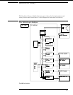
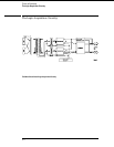
The probing circuit includes the probe cable and terminations. The probe cable consists of
two 17-channel pods which are connected to the circuit board using a high-density connector.
Sixteen single-ended data channels and one single-ended clock/data channel are passed to the
circuit board per pod.
If the clock/data channel is not used as a state clock in state acquisition mode, it is available as
a data channel. The clock/data channel is also available as a data channel in timing acquisition
mode. Two clock/data channels are available as data channels, and all clock data channels
available can be assigned as clock channels.
The cables use nichrome wire woven in polyarmid yarn for reliability and durability. The pods
also include one ground path per channel in addition to a pod ground. The channel grounds
are configured such that their electrical distance is the same as the electrical distance of the
channel.
The probe tip assemblies and termination modules connected at the end of the probe cables
have a divide-by-10 RC network that reduces the amplitude of the data signals as seen by the
circuit board. This adds flexibility to the types of signals the circuit board can read in addition
to improving signal integrity.
The terminations on the circuit board are resistive terminations that reduce transmission line
effects on the cable. The terminations also improve signal integrity to the comparators by
matching the impedance of the probe cable channels with the impedance of the signal paths of
the circuit board. All 17 channels of each pod are terminated in the same way. The signals
are still reduced by a factor of 10.
Comparators
Two proprietary 9-channel comparators per pod interpret the incoming data and clock signals
as either high or low depending on where the user-programmable threshold is set. The
threshold voltage of each pod is individually programmed, and the voltage selected applies to
the clock channel as well as the data channels of each pod.
Each of the comparator ICs has a serial test input port used for testing purposes. A test bit
pattern is sent from the Test and Clock Synchronization Circuit to the comparator. The
comparators then propagate the test signal on each of the nine channels of the comparator.
Consequently, all data and clock channel pipelines on the circuit board can be tested by the
operating system software from the comparator.
Acquisition
The acquisition circuit is made up of a single Agilent Technologies proprietary ASIC. Each
ASIC is a 34-channel state/timing analyzer, and one such ASIC is included for every two logic
analyzer pods. All of the sequencing, pattern/range recognition, and event counting functions
are performed on board the IC.
In addition to the storage qualification and counting functions, the acquisition ASICs also
perform master clocking functions. All six state acquisition clocks are fed to each IC, and the
ICs generate their own sample clocks. Every time you select RUN, the ICs individually
perform a clock optimization before data is stored.
Theory of Operation
The Logic Acquisition Circuitry
8–7