Analyzer Tests (Analy PV)
The analyzer tests are functional performance verification tests. There are three types of
analyzer tests: the Board Test, the Chip Test, and the Data Input Inspection. The following
describes the analyzer self-tests:
Board Test
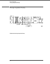
The Board Test functionally verifies the two oscillators and the 9-channel comparators on the
circuit board. First, the oscillators are checked using the event counter on one of the
acquisition ICs. The event counter will count the number of oscillator periods within a
pre-determined time window. The count of oscillator periods is then compared with a known
value.
The comparators are then checked by varying the threshold voltage and reading the state of
the activity indicators. The outputs of the octal DAC are set to the upper voltage limit and the
activity indicators for all of the pod channels are read to see if they are all in a low state.
The octal DAC outputs are then set to the lower voltage limit, and the activity indicators are
read to see if they are in a high state. The DAC outputs are then set to 0.0 V, allowing the
comparators to recognize the test signal being routed to the test input pin of all of the
comparators. Consequently, the activity indicators are read to see if they show activity on all
channels of all of the pods.
Chip Tests
During the Chip Tests, six tests are performed on the acquisition ICs. The tests are the
Communications, Memory, Encoder, Resource, Sequencer, and Clock Generation Tests.
Communications Test The communications test verifies that communications pipeline
between the various subsystems of the IC are operating. Checkerboard patterns of "1s"
and "0s" are routed to the address and data buses and to the read/write registers of each
chip. After verifying the communications pipelines, the acquisition clock synchronization
signals that are routed from IC to IC are checked. Finally, the IC master clock
optimization path is checked and verified.
Passing the communications test implies that the communications pipelines running from
subsystem to subsystem on the acquisition IC are functioning and that the clock optimization
circuit on the IC is functioning. Also, passing this test implies that the acquisition clock
synchronization signals are functioning and appear at the synchronization signal output pins
of the acquisition IC.
Memory Test Acquisition RAM is checked by filling the IC RAM with a checkerboard
pattern of "1s" and "0s," then reading each memory location and comparing the test
pattern with known values. Then, the IC RAM is filled with an inverse checkerboard
pattern, read, and compared with known values.
Passing the memory test implies that the acquisition IC RAM is functioning and that each
memory location bit can hold either a logical "1" or logical "0."
Encoder Test The encoder in the FISO front end is tested and verified using a walking
"1" and walking "0" pattern. The walking "1" and "0" is used to stimulate all of the encoder
output pins which connect directly to the FISO memory cells. Additionally, the post-store
counter in each of the acquisition ICs is tested.
Passing the encoder test implies that the FISO encoder is functioning and can properly route
the acquired data to the acquisition memory FISO RAM. Also, passing this test implies that
the post-store counter on the acquisition ICs is functioning.
Theory of Operation
Analyzer Tests (Analy PV)
8–13


