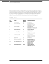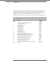
Resource Test The pattern, range, edge, and glitch recognizers are tested and verified.
First, the test register is verified for correct operation. Next, the pattern comparators are
tested to ensure that each bit in the recognizer memory location as well as the logic
driver/receiver are operating. The edge and glitch pattern detectors are then verified in a
similar manner. The range detectors are verified with their combinational logic to ensure
that the in- and out-of-range conditions are recognized.
Passing the resource test implies that all of the pattern, range, edge, and glitch resources are
operating and that an occurrence of the pattern, edge, or glitch of interest is recognized. Also,
passing this test implies that the range recognizers will detect and report in- and out-of-range
acquisition data to the sequencer or storage qualifier. The drivers and receivers at the
recognizer input and output pins of the acquisition IC are also checked to be sure they are
functioning.
Sequencer Test The sequencer, the state machine that controls acquisition storage, is
tested by first verifying that all of the sequencer registers are operating. After the
registers are checked, the combinational logic of the storage qualification is verified.
Then, both the occurrence counter and the sequencer level counter are checked.
Passing the sequencer test implies that all 12 available sequence levels are functioning and
that all possible sequence level jumps can occur. Also, passing this test implies that
user-defined ANDing and ORing of storage qualified data patterns will occur, and that the
occurrence counter that appears at each sequence level is functioning.
Clock Generator Test The master clock generator on the acquisition ICs is tested by
first checking the operation of the clock optimization circuit. The state acquisition clock
paths are then checked to ensure that each state clock and clock qualifier are operating
by themselves and in all possible clock and qualifier combinations. The timing acquisition
optimization circuit is then operationally verified. Finally, the timing acquisition
frequency divider (for slower timing sample rates) is checked.
Passing the clock generator test implies that each acquisition IC can generate its own master
clock whether the clock is generated using a combination of external clocking signals (state
mode) or internal sample clock signals (timing mode).
Data Input Inspection
The data input inspection allows a user to verify that all of the data and clock/data pipelines
are operational. When the data input inspection test is selected, a test signal is fed to the test
input pins of all 9-channel comparators. The test menu displays the activity indicators for all
data and clock/data channels, which should show transitioning data signals on all channels.
The data input inspection is not an active part of the performance verification. However, the
test is useful for identifying failed channels in order to temporarily work around the problem
until the logic analyzer module can be sent to an Agilent Technologies service center for
repair.
Theory of Operation
Analyzer Tests (Analy PV)
8–14


