


AMD Geode™ SC1200/SC1201 Processor Data Book 131
SuperI/O Module
32579B
5.8.2 UART Functionality (SP1 and SP2)
Both SP1 and SP2 provide UART functionality. The
generic SP1 and SP2 support serial data communication
with remote peripheral device or modem using a wired
interface. The functional blocks can function as a standard
16450, 16550, or as an Extended UART.
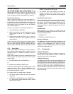
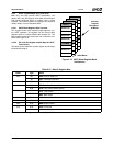
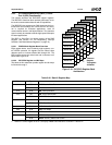
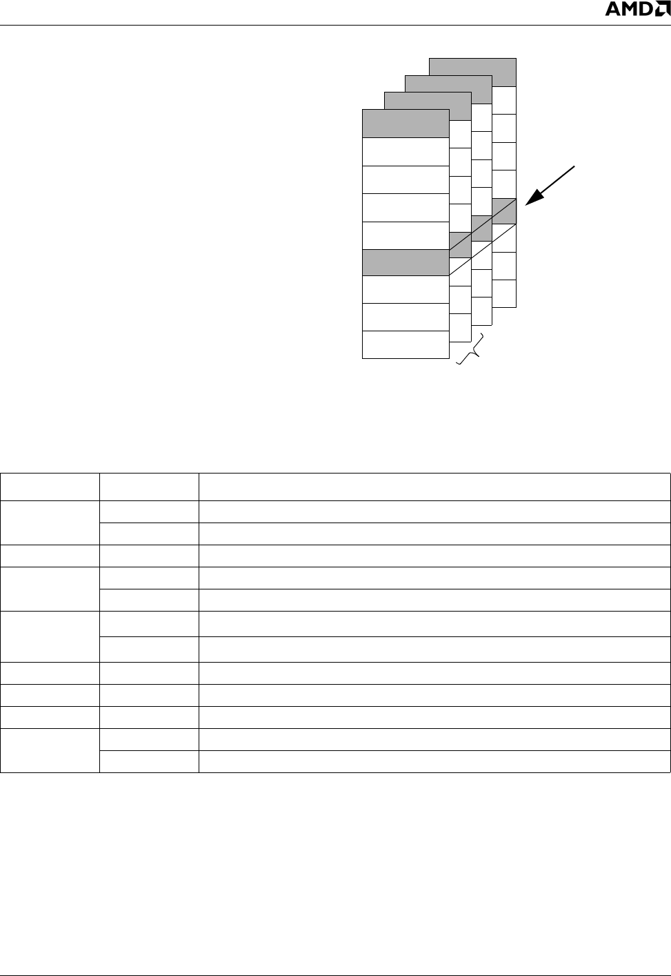
5.8.2.1 UART Mode Register Bank Overview
Four register banks, each containing eight registers, con-
trol UART operation. All registers use the same 8-byte
address space to indicate offsets 00h through 07h. The
BSR register selects the active bank and is common to all
banks. See Figure 5-18.
5.8.2.2 SP1 and SP2 Register and Bit Maps for UART
Functionality
The tables in this subsection provide register and bit maps
for Banks 0 through 3.
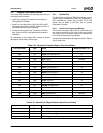
Figure 5-18. UART Mode Register Bank
Architecture
Bank 0
Bank 1
Bank 2
Bank 3
Offset 07h
Offset 06h
Offset 05h
Offset 04h
LCR/BSR
Offset 02h
Offset 01h
Offset 00h
Common
Register
Throughout
All Banks
16550 Banks
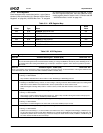
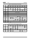
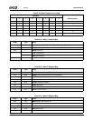
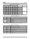
Table 5-37. Bank 0 Register Map
Offset Type Name
00h RO RXD. Receiver Data Port
W TXD. Transmitter Data Port
01h R/W IER. Interrupt Enable
02h RO EIR. Event Identification (Read Cycles)
R/W FCR. FIFO Control (Write Cycles)
03h W
LCR
1
. Line Control
R/W
BSR
1
.Bank Select
04h R/W MCR. Modem/Mode Control
05h R/W LSR. Link Status
06h R/W MSR. Modem Status
07h R/W SPR. Scratchpad
R/W ASCR. Auxiliary Status and Control
1. When bit 7 of this register is set to 1, bits [6:0] of BSR select the bank, as shown in Table 5-38 on page 132.