AMD Geode™ SC1200/SC1201 Processor Data Book 351
Video Processor Module - Video Processor Registers - Function 4
32579B
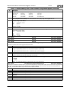
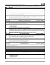
Offset 414h-417h VBI Horizontal Control Register (R/W) Reset Value: 00000000h
31:27 Reserved.
26:16 VBI_H_END (VBI Horizontal End). Specifies the horizontal end position for VBI data sent to the encoder.
15:11 Reserved.
10:0 VBI_H_START (VBI Horizontal Start). Specifies the horizontal start position for VBI data sent to the encoder.
Offset 418h-41Bh VBI Total Count Register - Odd (R/W) Reset Value: 00000000h
31:20 Reserved.
19:0 VBI_TOTAL_COUNT_ODD (VBI Odd Fields Total Count). Specifies the total count of VBI data in bytes for odd fields. This
field is used to separate VBI data from active video data when both types of data are received from the GX1 module’s video
port.
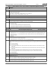
Offset 41Ch-41Fh VBI Total Count Register - Even (R/W) Reset Value: 00000000h
31:20 Reserved.
19:0 VBI_TOTAL_COUNT_EVEN (VBI Even Fields Total Count). Specifies the total count of VBI data in bytes for even fields.
This field is used to separate VBI data from active video data when both types of data are received from the GX1 module’s
video port.
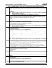
Offset 420h-423h GenLock Register (R/W) Reset Value: 00000000h
31:24 Reserved. Must be set to 0.
23 ODD_TO (Odd Field Time Out). Indicates CGENTO0 (F4BAR0+Memory Offset 43Ch[15:0]) has expired. This bit can be
reset by writing 1 to it.
22 EVEN_TO (Even Field Time Out). Indicates CGENTO1 (F4BAR0+Memory Offset 43Ch[31:16]) has expired. This bit can
be reset by writing 1 to it.
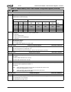
21:9 Reserved.
8 GENLOCK_TO_ENC_TIMING (GenLock to Encoder Timing). Selects the timing to which the GX1 module’s vertical tim-
ing needs to be synchronized.
0: VIP vertical timing.
1: Encoder vertical timing. The TV encoder generates a reference for GenLock at the start of line 1 of its counters.
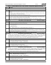
7 Reserved. Set to 0.
6 RST_ENC_BFOR_DLY (Reset Encoder Before Delay). Selects the position of the encoder reset with respect to the pro-
grammed VIP_VSYNC edge and delay.
0: The encoder is reset after the programmed delay.
1: The encoder is reset before the programmed delay.
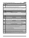
5 FIELD_EVEN (Encoder Field Even). Used in conjunction with bit 0 of this register for single GenLock field synchronization.
0: Encoder field is set to odd.
1: Encoder field is set to even.
4 GENLOCK_TOUT_EN (GenLock Timeout Enable).
0: Disable.
1: Enable timeout.
3 VIP_VSYNC_EDGE_SEL (VIP VSYNC Edge Select). Selects which edge of the VSYNC signal should be synchronized
with VIP.
0: Rising edge.
1: Falling edge.
2 GX1_VSYNC_EDGE_SEL (GX1 VSYNC Edge Select). Selects which edge of the VSYNC signal should be synchronized
with the GX1 module.
0: Rising edge.
1: Falling edge.
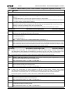
Table 7-9. F4BAR0+Memory Offset: Video Processor Configuration Registers (Continued)
Bit Description


