AMD Geode™ SC1200/SC1201 Processor Data Book 377
Electrical Specifications
32579B
9.3.1 Memory Controller Interface
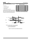
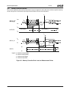
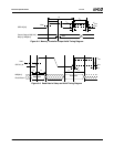
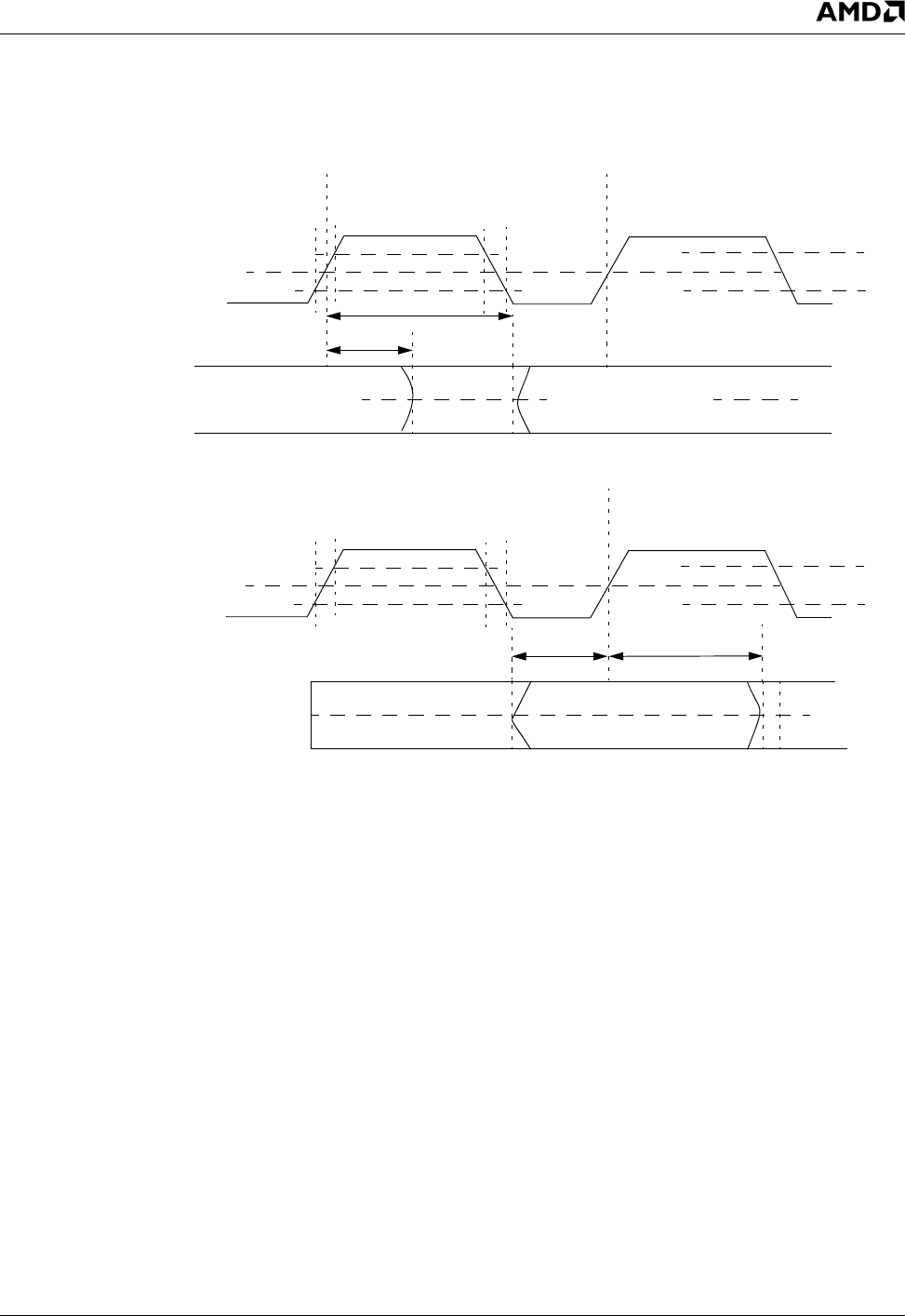
The minimum input setup and hold times described in Figure 9-3 (legend C and D) define the smallest acceptable sampling
window during which a synchronous input signal must be stable to ensure correct operation.
Figure 9-3. Memory Controller Drive Level and Measurement Points
SDCLK_OUT
V
OH
V
REF
V
REF
V
REF
C
Valid Output
n+1
A
B
Valid Output
n
OUTPUTS
INPUTS
V
IH
V
IL
V
OL
Min
Max
Legend: A = Maximum Output Delay
B = Minimum Output Delay
C = Minimum Input Setup
D = Minimum Input Hold
D
t
x
V
OH
V
OL
V
OLD
V
OHD
SDCLK_IN
V
IH
V
REF
V
IL
t
x
V
ILD
V
IHD
SDCLK[3:0]


