AMD Geode™ SC1200/SC1201 Processor Data Book 87
General Configuration Block
32579B
4.5.7 Clock Registers
The clock generator and PLL registers are described in Table 4-8.
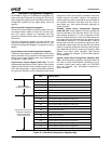
Table 4-8. Clock Generator Configuration
Bit Description
Offset 10h Maximum Core Clock Multiplier Register - MCCM (RO) Reset Value: Strapped Value
This register holds the maximum core clock multiplier value. The maximum clock frequency allowed by the core, is the Fast-PCI clock
multiplied by this value.
7:4 Reserved.
3:0 MCM (Maximum Clock Multiplier). This 4-bit value is the maximum multiplier value allowed for the core clock generator. It
is derived from strap pins CLKSEL[3:0] based on the multiplier value in Table 4-7 on page 85.
Offset 11h Reserved - RSVD
Offset 12h PLL Power Control Register - PPCR (R/W) Reset Value: 2Fh
This register controls operation of the PLLs.
7 Reserved.
6 EXPCID (Disable External PCI Clock).
0: External PCI clock is enabled.
1: External PCI clock is disabled.
5 GPD (Disable Graphic Pixel Reference Clock).
0: PLL2 input clock is enabled.
1: PLL2 input clock is disabled.
4 Reserved.
3 PLL3SD (Shut Down PLL3). AC97 codec clock.
0: PLL3 is enabled.
1: PLL3 is shutdown.
2 FM1SD (Shut Down PLL4).
0: PLL4 is enabled.
1: PLL4 is shutdown, unless internal Fast-PCI clock is strapped to 48 MHz.
1 C48MD (Disable SuperI/O and USB Clock).
0: USB and SuperI/O clock is enabled.
1: USB and SuperI/O clock is disabled.
0 Reserved. Write as read.
Offset 13h-17h Reserved - RSVD
Offset 18h-1Bh PLL3 Configuration Register - PLL3C (R/W) Reset Value: E1040005h
31:24 MFFC (MFF Counter Value).
Fvco = OSCCLK * MFBC / (MFFC * MOC)
OSCCLK = 27 MHz
23:19 Reserved. Write as read.
18:8 MFBC (MFB Counter Value).
Fvco = OSCCLK * MFBC / (MFFC * MOC)
OSCCLK = 27 MHz
Note: Bits 18, 9, and 8 cannot be changed. Bit 18 is always a 1; bits 9 and 8 are always 0.
7 Reserved. Write as read.
6 Reserved. Must be set to 0.
5:0 MOC (MO Counter Value).
Fvco = OSCCLK * MFBC / (MFFC * MOC)
OSCCLK = 27 MHz


