210 AMD Geode™ SC1200/SC1201 Processor Data Book
Core Logic Module - Bridge, GPIO, and LPC Registers - Function 0
32579B
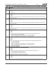
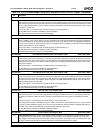
Index 87h Second Level PME/SMI Status Mirror Register 4 (RO) Reset Value: 00h
The bits in this register contain second level status reporting. Top level status is reported at F1BAR0+I/O Offset 00h/02h[0].
This register is called a “Mirror” register since an identical register exists at F0 Index F7h. Reading this register does not clear the status,
while reading its counterpart at F0 Index F7h clears the status at both the second and top levels except for bit 7 which has a third level of
SMI status reporting at F0BAR0+I/O 0Ch/1Ch.
7 GPIO Event SMI Status. Indicates whether or not an SMI was caused by a transition of any of the GPIOs (GPIO47-GPIO32
and GPIO15-GPIO0).
0: No.
1: Yes.
To enable SMI generation, set F1BAR1+I/O Offset 0Ch[0] to 0.
F0BAR0+I/O Offset 08h/18h selects which GPIOs are enabled to generate a PME and setting F1BAR1+I/O Offset 0Ch[0] =
0 enables the PME to generate an SMI. In addition, the selected GPIO must be enabled as an input (F0BAR0+I/O Offset
20h and 24h).
The next level (third level) of SMI status is at F0BAR0+I/O 0Ch/1Ch[15:0].
6 Thermal Override SMI Status. Indicates whether or not an SMI was caused by the assertion of THRM#.
0: No.
1: Yes.
To enable SMI generation, set F0 Index 83h[4] to 1.
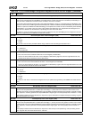
5:4 Reserved. Always reads 0.
3 SIO PWUREQ SMI Status. Indicates whether or not an SMI was caused by a power-up event from the SIO.
0: No.
1: Yes.
A power-up event is defined as any of the following events/activities:
— RI2#
— SDATA_IN2
— IRRX1 (CEIR)
To enable SMI generation, set F1BAR1+I/O Offset 0Ch[0] to 0.
2 Codec SDATA_IN SMI Status. Indicates whether or not an SMI was caused by AC97 Codec producing a positive edge on
SDATA_IN.
0: No.
1: Yes.
To enable SMI generation, set F0 Index 80h[5] to 1.
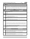
1 RTC Alarm (IRQ8#) SMI Status. Indicates whether or not an SMI was caused by an RTC interrupt.
0: No.
1: Yes.
This SMI event can only occur while in 3V Suspend and an RTC interrupt occurs with F1BAR1+I/O Offset 0Ch[0] = 0.
0 ACPI Timer SMI Status. Indicates whether or not an SMI was caused by an ACPI Timer (F1BAR0+I/O Offset 1Ch or
F1BAR1+I/O Offset 1Ch) MSB toggle.
0: No.
1: Yes.
To enable SMI generation, set F0 Index 83h[5] to 1.
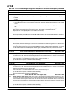
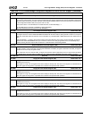
Index 88h General Purpose Timer 1 Count Register (R/W) Reset Value: 00h
7:0 GPT1_COUNT. This field represents the load value for General Purpose Timer 1. This value can represent either an 8-bit
counter or a 16-bit counter (selected in F0 Index 8Bh[4]). It is loaded into the counter when the timer is enabled (F0 Index
83h[0] = 1). Once enabled, an enabled event (configured in F0 Index 89h[6:0]) reloads the timer.
The counter is decremented with each clock of the configured timebase (1 msec or 1 sec selected at F0 Index 89h[7]). Upon
expiration of the counter, an SMI is generated, and the top level SMI status is reported at F1BAR0+I/O Offset 00h/02h[9].
The second level SMI status is reported at F1BAR0+I/O Offset 04h/06h[0]. Once expired, this counter must be re-initialized
by either disabling and enabling it, or writing a new count value in this register. See Section 6.2.10.3 "Peripheral Power Man-
agement" on page 164 for a discussion on the limitations of producing count error with small values.
Table 6-29. F0: PCI Header/Bridge Configuration Registers for GPIO and LPC Support (Continued)
Bit Description


