AMD Geode™ SC1200/SC1201 Processor Data Book 21
Architecture Overview
32579B
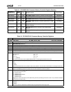
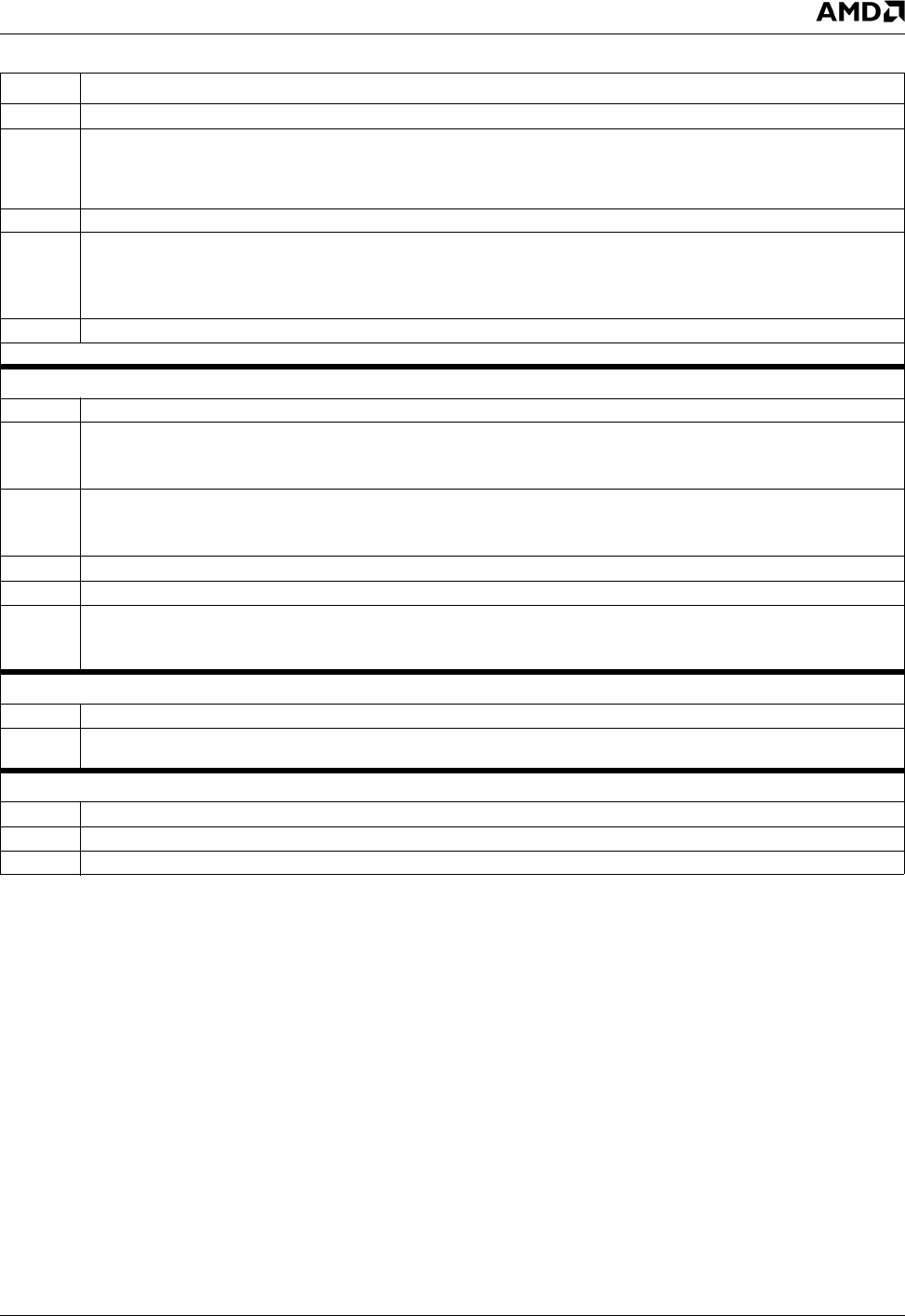
11 RSVD (Reserved). Write as 0.
10:8 RRD (ACT(0) to ACT(1) Command Period, tRRD). Minimum number of SDRAM clocks between ACT and ACT command
to two different component banks within the same module bank. The memory controller does not perform back-to-back Acti-
vate commands to two different component banks without a READ or WRITE command between them. Hence, this field
should be written as 001.
7 RSVD (Reserved). Write as 0.
6:4 DPL (Data-in to PRE Command Period, tDPL). Minimum number of SDRAM clocks from the time the last write datum is
sampled till the bank is precharged:
000: Reserved 010: 2 CLK 100: 4 CLK 110: 6 CLK
001: 1 CLK 011: 3 CLK 101: 5 CLK 111: 7 CLK
3:0 RSVD (Reserved). Leave unchanged. Always returns a 101h.
Note: Refer to the SDRAM manufacturer’s specification for more information on component banks.
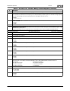
GX_BASE+8414h-8417h MC_GBASE_ADD (R/W) Reset Value: 00000000h
31:18 RSVD (Reserved). Write as 0.
17 TE (Test Enable TEST[3:0]).
0: TEST[3:0] are driven low (normal operation).
1: TEST[3:0] pins are used to output test information
16 TECTL (Test Enable Shared Control Pins).
0: RASB#, CASB#, CKEB, WEB# (normal operation).
1: RASB#, CASB#, CKEB, WEB# are used to output test information
15:12 SEL (Select). This field is used for debug purposes only and should be left at zero for normal operation.
11 RSVD (Reserved). Write as 0.
10:0 GBADD (Graphics Base Address). This field indicates the graphics memory base address, which is programmable on 512
KB boundaries. This field corresponds to address bits [29:19].
Note that BC_DRAM_TOP must be set to a value lower than the Graphics Base Address.
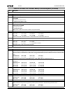
GX_BASE+8418h-841Bh MC_DR_ADD (R/W) Reset Value: 00000000h
31:10 RSVD (Reserved). Write as 0.
9:0 DRADD (Dirty RAM Address). This field is the address index that is used to access the Dirty RAM with the MC_DR_ACC
register. This field does not auto increment.
GX_BASE+841Ch-841Fh MC_DR_ACC (R/W) Reset Value: 0000000xh
31:2 RSVD (Reserved). Write as 0.
1 D (Dirty Bit). This bit is read/write accessible.
0 V (Valid Bit). This bit is read/write accessible.
Table 2-2. SC1200/SC1201 Processor Memory Controller Registers (Continued)
Bit Description


