214 AMD Geode™ SC1200/SC1201 Processor Data Book
Core Logic Module - Bridge, GPIO, and LPC Registers - Function 0
32579B
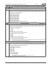
Index 96h Suspend Configuration Register (R/W) Reset Value: 00h
7:3 Reserved. Must be set to 0.
2 Suspend Mode Configuration. Special 3V Suspend mode to support powering down the GX1 module during Suspend.
0: Disable.
1: Enable.
1 SMI Speedup Configuration. Selects how the Suspend Modulation function should react when an SMI occurs.
0: Use the IRQ Speedup Timer Count Register (F0 Index 8Ch) to temporarily disable Suspend Modulation when an SMI
occurs.
1: Disable Suspend Modulation when an SMI occurs until a read to the SMI Speedup Disable Register (F1BAR0+I/O Offset
08h).
The purpose of this bit is to disable Suspend Modulation while the GX1 module is in the System Management Mode so that
VSA and Power Management operations occur at full speed. Two methods for accomplishing this are:
Map the SMI into the IRQ Speedup Timer Count Register (F0 Index 8Ch).
- or -
Have the SMI disable Suspend Modulation until the SMI handler reads the SMI Speedup Disable Register (F1BAR0+I/O
Offset 08h). This the preferred method.
This bit has no affect if the Suspend Modulation feature is disabled (bit 0 = 0).
0 Suspend Modulation Feature Enable. This bit is used to enable/disable the Suspend Modulation feature.
0: Disable.
1: Enable.
When enabled, the internal SUSP# signal is asserted and de-asserted for the durations programmed in the Suspend Modu-
lation register (F0 Index 94h).
The setting of this bit is mirrored in the Top Level PME/SMI Status register (F1BAR0+I/O Offset 00h/02h[15]. It is used by
the SMI handler to determine if the SMI Speedup Disable register (F1BAR0+I/O Offset 08h) must be cleared on exit.
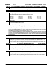
Index 97h Reserved Reset Value: 00h
Index 98h-99h Primary Hard Disk Idle Timer Count Register (Primary Channel) (R/W) Reset Value: 0000h
15:0 Primary Hard Disk Idle Timer Count. This idle timer is used to determine when the primary hard disk is not in use so that
it can be powered down. The 16-bit value programmed here represents the period of hard disk inactivity after which the sys-
tem is alerted via an SMI. The timer is automatically reloaded with the count value whenever an access occurs to the config-
ured hard disk’s data port (I/O port 1F0h or 3F6h).
This counter uses a 1 second timebase. To enable this timer, set F0 Index 81h[0] = 1.
Top level SMI status is reported at F1BAR0+I/O Offset 00h/02h[0].
Second level SMI status is reported at F0 Index 85h/F5h[0].
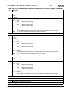
Index 9Ah-9Bh Floppy Disk Idle Timer Count Register (R/W) Reset Value: 0000h
15:0 Floppy Disk Idle Timer Count. This idle timer is used to determine when the floppy disk drive is not in use so that it can be
powered down. The 16-bit value programmed here represents the period of floppy disk drive inactivity after which the sys-
tem is alerted via an SMI. The timer is automatically reloaded with the count value whenever an access occurs to the config-
ured floppy drive’s data port (I/O port 3F5h or 375h).
This counter uses a 1 second time base. To enable this timer, set F0 Index 81h[1] = 1.
Top level SMI status is reported at F1BAR0+I/O Offset 00h/02h[0].
Second level SMI status is reported at F0 Index 85h/F5h[1].
Index 9Ch-9Dh Parallel / Serial Idle Timer Count Register (R/W) Reset Value: 0000h
15:0 Parallel / Serial Idle Timer Count. This idle timer is used to determine when the parallel and serial ports are not in use so
that the ports can be power managed. The 16-bit value programmed in this register represents the period of inactivity for
these ports after which the system is alerted via an SMI. The timer is automatically reloaded with the count value whenever
an access occurs to the parallel (LPT) or serial (COM) I/O address spaces. If the mouse is enabled on a serial port, that port
is not considered here.
This counter uses a 1 second timebase. To enable this timer, set F0 Index 81h[2] = 1.
Top level SMI status is reported at F1BAR0+I/O Offset 00h/02h[0].
Second level SMI status is reported at F0 Index 85h/F5h[2].
Table 6-29. F0: PCI Header/Bridge Configuration Registers for GPIO and LPC Support (Continued)
Bit Description


